SBOS948F February 2019 – May 2021 BUF634A
PRODUCTION DATA
- 1 Features
- 2 Applications
- 3 Description
- 4 Revision History
- 5 Device Comparison Table
- 6 Pin Configuration and Functions
- 7 Specifications
- 8 Detailed Description
- 9 Application and Implementation
- 10Power Supply Recommendations
- 11Layout
- 12Device and Documentation Support
- 13Mechanical, Packaging, and Orderable Information
Package Options
Refer to the PDF data sheet for device specific package drawings
Mechanical Data (Package|Pins)
- D|8
- DDA|8
- DRB|8
Thermal pad, mechanical data (Package|Pins)
Orderable Information
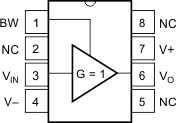
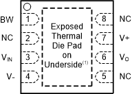
6 Pin Configuration and Functions
 Figure 6-1 D and DDA Packages8-Pin SOIC, 8-Pin HSOIC with Thermal
PadTop View
 Figure 6-2 DRB Package8-Pin VSON with Thermal PadTop
View
Figure 6-2 DRB Package8-Pin VSON with Thermal PadTop
ViewTable 6-1 Pin Functions
| PIN | I/O(2) | DESCRIPTION | |||
|---|---|---|---|---|---|
| NAME | DDA(1) | DRB(1) | D | ||
| BW | 1 | 1 | 1 | I | Bandwidth adjust pin. Connect the BW pin to the V– pin for wide-BW mode and leave the BW pin floating for low-IQ mode. See the Adjustable Bandwidth section. |
| NC | 2, 5, 8 | 2, 5, 8 | 2, 5, 8 | — | No internal connection |
| V– | 4 | 4 | 4 | P | Negative power supply |
| V+ | 7 | 7 | 7 | P | Positive power supply |
| VIN | 3 | 3 | 3 | I | Input |
| VO | 6 | 6 | 6 | O | Output |
| Thermal Pad | — | — | Thermal pad. Must be electrically shorted to V–. | ||
(1) The DRB and DDA packages include a thermal pad on the backside
of the device. The thermal pad must be connected to the same potential as V–.
Connect the thermal pad and V– to a heat-spreading plane to achieve low thermal
impedance. The thermal pad can also be unused (not connected to any
heat-spreading plane or voltage), thus giving an overall higher thermal
impedance.
(2) I = input, O = output, P = power.