SBAS528D June   2013  – December 2021 DAC7760 , DAC8760

PRODUCTION DATA  

  1. Features
  2. Applications
  3. Description
  4. Revision History
  5. Device Comparison Table
  6. Pin Configuration and Functions
  7. Specifications
    1. 7.1  Absolute Maximum Ratings
    2. 7.2  ESD Ratings
    3. 7.3  Recommended Operating Conditions
    4. 7.4  Thermal Information
    5. 7.5  Electrical Characteristics
    6. 7.6  Electrical Characteristics: AC
    7. 7.7  Timing Requirements: Write Mode
    8. 7.8  Timing Requirements: Readback Mode
    9. 7.9  Timing Diagrams
    10. 7.10 Typical Characteristics
  8. Detailed Description
    1. 8.1 Overview
    2. 8.2 Functional Block Diagram
    3. 8.3 Feature Description
      1. 8.3.1  DAC Architecture
      2. 8.3.2  Voltage Output Stage
      3. 8.3.3  Current Output Stage
      4. 8.3.4  Internal Reference
      5. 8.3.5  Digital Power Supply
      6. 8.3.6  DAC Clear
      7. 8.3.7  Power-On Reset
      8. 8.3.8  Alarm Detection
      9. 8.3.9  Watchdog Timer
      10. 8.3.10 Frame Error Checking
      11. 8.3.11 User Calibration
      12. 8.3.12 Programmable Slew Rate
    4. 8.4 Device Functional Modes
      1. 8.4.1 Setting Voltage and Current Output Ranges
      2. 8.4.2 Boost Configuration for IOUT
      3. 8.4.3 Filtering the Current Output (only on the VQFN package)
      4. 8.4.4 HART Interface
        1. 8.4.4.1 For 4-mA to 20-mA Mode
        2. 8.4.4.2 For All Current Output Modes
    5. 8.5 Programming
      1. 8.5.1 Serial Peripheral Interface (SPI)
        1. 8.5.1.1 SPI Shift Register
        2. 8.5.1.2 Write Operation
        3. 8.5.1.3 Read Operation
        4. 8.5.1.4 Stand-Alone Operation
        5. 8.5.1.5 Multiple Devices on the Bus
    6. 8.6 Register Maps
      1. 8.6.1 DACx760 Command and Register Map
        1. 8.6.1.1 DACx760 Register Descriptions
          1. 8.6.1.1.1 Control Register
          2. 8.6.1.1.2 Configuration Register
          3. 8.6.1.1.3 DAC Registers
          4. 8.6.1.1.4 Reset Register
          5. 8.6.1.1.5 Status Register
  9. Application and Implementation
    1. 9.1 Application Information
      1. 9.1.1 Controlling the VOUT and IOUT Pins
        1. 9.1.1.1 VOUT and IOUT Pins are Independent Outputs, Never Simultaneously Enabled
        2. 9.1.1.2 VOUT and IOUT Pins are Independent Outputs, Simultaneously Enabled
        3. 9.1.1.3 VOUT and IOUT Pins are Tied Together, Never Simultaneously Enabled
      2. 9.1.2 Implementing HART in All Current Output Modes
        1. 9.1.2.1 Using CAP2 Pin on VQFN Package
        2. 9.1.2.2 Using the ISET-R Pin
      3. 9.1.3 Short-Circuit Current Limiting
    2. 9.2 Typical Application
      1. 9.2.1 Design Requirements
      2. 9.2.2 Detailed Design Procedure
      3. 9.2.3 Application Curves
  10. 10Power Supply Recommendations
  11. 11Layout
    1. 11.1 Layout Guidelines
      1. 11.1.1 Thermal Considerations
    2. 11.2 Layout Example
  12. 12Device and Documentation Support
    1. 12.1 Documentation Support
      1. 12.1.1 Related Documentation
    2. 12.2 Receiving Notification of Documentation Updates
    3. 12.3 Support Resources
    4. 12.4 Trademarks
    5. 12.5 Electrostatic Discharge Caution
    6. 12.6 Glossary
  13. 13Mechanical, Packaging, and Orderable Information

Package Options

Mechanical Data (Package|Pins)
Thermal pad, mechanical data (Package|Pins)
Orderable Information

Description

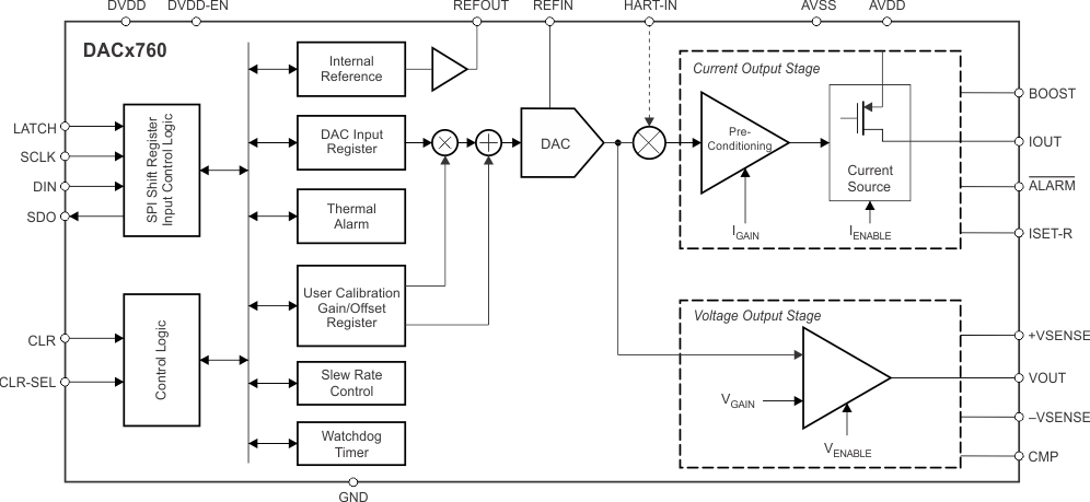
TheDACx760 are precision, fully integrated, 12-bit and 16-bit digital-to-analog converters (DACs) designed to meet the requirements of industrial process-control applications. These devices are programmable as a current output with a range of 4 mA to 20 mA, 0 mA to 20 mA, or 0 mA to 24 mA; or as a voltage output with a range of 0 V to 5 V, 0 V to 10 V, ±5 V, or ±10 V with a 10% overrange (0 V to 5.5 V, 0 V to 11 V, ±5.5 V, or ±11 V). Both current and voltage outputs can be simultaneously enabled while being controlled by one data register.

These devices include a power-on-reset function for powering up in a known state (both IOUT and VOUT are disabled and in a Hi-Z state). The CLR and CLR-SEL pins set the voltage outputs to zero-scale or midscale, and the current output to the low end of the range if the output is enabled. Zero and gain registers can be programmed to digitally calibrate the device in the end system. The output slew rate is also programmable by register. These devices can superimpose an external HART® signal on the current output, and operate with either a single 10-V to 36-V supply, or dual supplies of up to ±18 V.

Device Information
PART NUMBERPACKAGE(1)BODY SIZE (NOM)
DACx760HTSSOP (24)7.80 mm × 4.40 mm
VQFN (40)6.00 mm × 6.00 mm
For all available packages, see the package option addendum at the end of the data sheet.
GUID-20211207-SS0I-ZWGJ-G5HK-DBKZCQMQNH3C-low.gif Block Diagram