DLPS132 May   2018 DLPA4000

PRODUCTION DATA.  

  1. Features
  2. Applications
  3. Description
    1.     Device Images
      1.      System Block Diagram
  4. Revision History
  5. Pin Configuration and Functions
    1.     Pin Functions
  6. Specifications
    1. 6.1 Absolute Maximum Ratings
    2. 6.2 ESD Ratings
    3. 6.3 Recommended Operating Conditions
    4. 6.4 Thermal Information
    5. 6.5 Electrical Characteristics
    6. 6.6 SPI Timing Parameters
  7. Detailed Description
    1. 7.1 Overview
    2. 7.2 Functional Block Description
    3. 7.3 Feature Description
      1. 7.3.1 Supply and Monitoring
        1. 7.3.1.1 Supply
        2. 7.3.1.2 Monitoring
          1. 7.3.1.2.1 Block Faults
          2. 7.3.1.2.2 Low Battery and UVLO
          3. 7.3.1.2.3 Thermal Protection
      2. 7.3.2 Illumination
        1. 7.3.2.1 Programmable Gain Block
        2. 7.3.2.2 LDO Illumination
        3. 7.3.2.3 Illumination Driver A
        4. 7.3.2.4 External MOSFETs
          1. 7.3.2.4.1 Gate series resistor (RG)
          2. 7.3.2.4.2 Gate series diode (DG)
          3. 7.3.2.4.3 Gate parallel capacitance (CG)
        5. 7.3.2.5 RGB Strobe Decoder
          1. 7.3.2.5.1 Break Before Make (BBM)
          2. 7.3.2.5.2 Openloop Voltage
          3. 7.3.2.5.3 Transient Current Limit
        6. 7.3.2.6 Illumination Monitoring
          1. 7.3.2.6.1 Power Good
          2. 7.3.2.6.2 RatioMetric Overvoltage Protection
      3. 7.3.3 External Power MOSFET Selection
        1. 7.3.3.1 Threshold Voltage
        2. 7.3.3.2 Gate Charge and Gate Timing
        3. 7.3.3.3 On-resistance RDS(on)
      4. 7.3.4 DMD Supplies
        1. 7.3.4.1 LDO DMD
        2. 7.3.4.2 DMD HV Regulator
        3. 7.3.4.3 DMD/DLPC Buck Converters
        4. 7.3.4.4 DMD Monitoring
          1. 7.3.4.4.1 Power Good
          2. 7.3.4.4.2 Overvoltage Fault
      5. 7.3.5 Buck Converters
        1. 7.3.5.1 LDO Bucks
        2. 7.3.5.2 General Purpose Buck Converters
        3. 7.3.5.3 Buck Converter Monitoring
          1. 7.3.5.3.1 Power Good
          2. 7.3.5.3.2 Overvoltage Fault
      6. 7.3.6 Auxiliary LDOs
      7. 7.3.7 Measurement System
    4. 7.4 Device Functional Modes
    5. 7.5 Programming
      1. 7.5.1 SPI
      2. 7.5.2 Interrupt
      3. 7.5.3 Fast-Shutdown in Case of Fault
      4. 7.5.4 Protected Registers
      5. 7.5.5 Writing to EEPROM
    6. 7.6 Register Maps
  8. Application and Implementation
    1. 8.1 Application Information
    2. 8.2 Typical Application
      1. 8.2.1 Design Requirements
      2. 8.2.2 Detailed Design Procedure
        1. 8.2.2.1 Component Selection for General-Purpose Buck Converters
    3. 8.3 System Example With DLPA4000 Internal Block Diagram
  9. Power Supply Recommendations
    1. 9.1 Power-Up and Power-Down Timing
  10. 10Layout
    1. 10.1 Layout Guidelines
      1. 10.1.1 LED Driver
        1. 10.1.1.1 PowerBlock Gate Control Isolation
        2. 10.1.1.2 VIN to PowerBlocks
        3. 10.1.1.3 Return Current from LEDs and RSense
        4. 10.1.1.4 RC Snubber
        5. 10.1.1.5 Capacitor Choice
      2. 10.1.2 General Purpose Buck 2
      3. 10.1.3 SPI Connections
      4. 10.1.4 RLIM Routing
      5. 10.1.5 LED Connection
    2. 10.2 Layout Example
    3. 10.3 Thermal Considerations
  11. 11Device and Documentation Support
    1. 11.1 Device Support
      1. 11.1.1 Device Nomenclature
    2. 11.2 Receiving Notification of Documentation Updates
    3. 11.3 Community Resources
    4. 11.4 Trademarks
    5. 11.5 Electrostatic Discharge Caution
    6. 11.6 Glossary
  12. 12Mechanical, Packaging, and Orderable Information
    1. 12.1 Package Option Addendum
      1. 12.1.1 Packaging Information

Package Options

Mechanical Data (Package|Pins)
Thermal pad, mechanical data (Package|Pins)
Orderable Information

Supply

The specified input supply voltage for main supply (VIN) is between 16 V and 20 V. The typical specification is 19.5 V. When the device energizes, several internal power supplies become energized sequentially.(Figure 1). A sequential startup ensures that all the different blocks start in a certain order and prevent excessive startup currents. The main control to start the device is the control pin PROJ_ON. Once set high the basic analog circuitry is started that is needed to operate the digital and SPI interface. This circuitry is supplied by two LDO regulators that generate 2.5 V (SUP_2P5V) and 5 V (SUP_5P0V). These regulator voltages internal only. Do not load these regulator voltages externally. Make sure the output capacitance is 2.2 µF for the 2.5-V LDO (pin 91) and 4.7 µF for the 5-V LDO, (pin 92). After the LDO voltages reach the regulator levels, the digital core starts, and the Digital State Machine (DSM) controls the device.

Subsequently, the 5.5-V LDOs for various blocks start: PWR_5V5V, DRST_5P5V and ILLUM_5P5V. Then the DLPC buck converters (PWR_1 & PWR_2) start and followed by the DMD LDOs (PWR_3 & PWR_4).The device enables and is controllable by the DLPC (indicated by RESET_Z going high). At this point the general purpose buck converter (PWR_6) can start. Lastly the regulator that supplies the DMD starts. The DMD regulator generates the timing critical VOFFSET, VBIAS, and VRESET supplies.
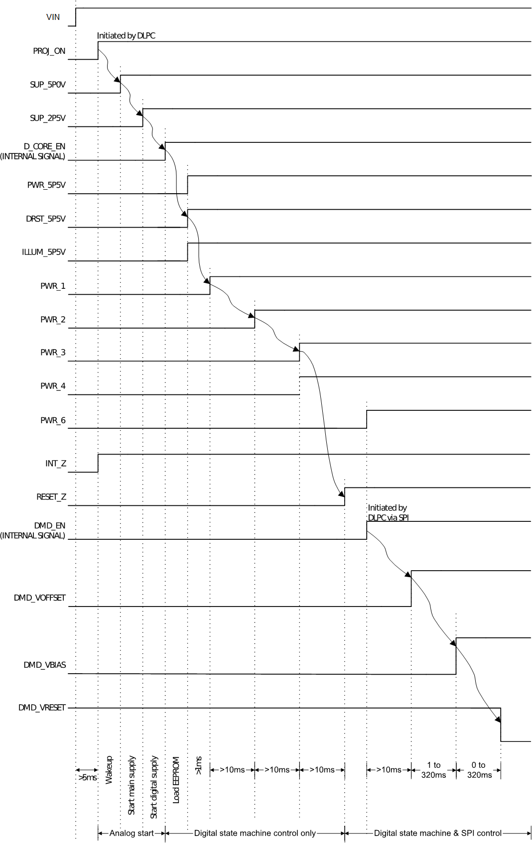
DLPA4000 DLPA4000_Powerup_Timing.gif

NOTE:

Arrows indicate sequence of events automatically controlled by digital state machine. Other events are initiated under SPI control.
Figure 1. Powerup Timing