DLPS031C December   2013  – August 2015 DLPC6401

PRODUCTION DATA.  

  1. Features
  2. Applications
  3. Description
    1.     Device Images
      1.      Typical Application Diagram
  4. Revision History
  5. Pin Configuration and Functions
    1.     Pin Functions
  6. Specifications
    1. 6.1  Absolute Maximum Ratings
    2. 6.2  ESD Ratings
    3. 6.3  Recommended Operating Conditions
    4. 6.4  Thermal Information
    5. 6.5  Electrical Characteristics
    6. 6.6  Electrical Characteristics (Normal Mode)
    7. 6.7  System Oscillators Timing Requirements
    8. 6.8  Test and Reset Timing Requirements
    9. 6.9  JTAG Interface: I/O Boundary Scan Application Timing Requirements
    10. 6.10 Port 1 Input Pixel Interface Timing Requirements
    11. 6.11 Port 2 Input Pixel Interface (FPD-Link Compatible LVDS Input) Timing Requirements
    12. 6.12 Synchronous Serial Port (SSP) Interface Timing Requirements
    13. 6.13 Programmable Output Clocks Switching Characteristics
    14. 6.14 Synchronous Serial Port (SSP) Interface Switching Characteristics
    15. 6.15 JTAG Interface: I/O Boundary Scan Application Switching Characteristics
  7. Detailed Description
    1. 7.1 Overview
    2. 7.2 Functional Block Diagram
    3. 7.3 Feature Description
      1. 7.3.1 System Reset Operation
        1. 7.3.1.1 Power-Up Reset Operation
        2. 7.3.1.2 System Reset Operation
        3. 7.3.1.3 Spread Spectrum Clock Generator Support
        4. 7.3.1.4 GPIO Interface
        5. 7.3.1.5 Source Input Blanking
        6. 7.3.1.6 Video and Graphics Processing Delay
      2. 7.3.2 Program Memory Flash/SRAM Interface
        1. 7.3.2.1 Calibration and Debug Support
        2. 7.3.2.2 Board-Level Test Support
    4. 7.4 Device Functional Modes
  8. Application and Implementation
    1. 8.1 Application Information
    2. 8.2 Typical Application
      1. 8.2.1 Design Requirements
        1. 8.2.1.1 Recommended MOSC Crystal Oscillator Configuration
      2. 8.2.2 Detailed Design Procedure
      3. 8.2.3 Application Curve
  9. Power Supply Recommendations
    1. 9.1 System Power Regulation
    2. 9.2 System Power-Up Sequence
    3. 9.3 Power-On Sense (POSENSE) Support
    4. 9.4 System Environment and Defaults
      1. 9.4.1 DLPC6401 System Power-Up and Reset Default Conditions
      2. 9.4.2 1.2-V System Power
      3. 9.4.3 1.8-V System Power
      4. 9.4.4 1.9-V System Power
      5. 9.4.5 3.3-V System Power
      6. 9.4.6 FPD-Link Input LVDS System Power
      7. 9.4.7 Power Good (PWRGOOD) Support
      8. 9.4.8 5-V Tolerant Support
  10. 10Layout
    1. 10.1 Layout Guidelines
      1. 10.1.1 PCB Layout Guidelines for Internal ASIC Power
      2. 10.1.2 PCB Layout Guidelines for Quality Auto-Lock Performance
      3. 10.1.3 DMD Interface Considerations
      4. 10.1.4 General Handling Guidelines for Unused CMOS-Type Pins
    2. 10.2 Layout Example
    3. 10.3 Thermal Considerations
  11. 11Device and Documentation Support
    1. 11.1 Device Support
      1. 11.1.1 Device Nomenclature
        1. 11.1.1.1 Video Timing Parameter Definitions
        2. 11.1.1.2 Device Marking
    2. 11.2 Community Resources
    3. 11.3 Trademarks
    4. 11.4 Electrostatic Discharge Caution
    5. 11.5 Glossary
  12. 12Mechanical, Packaging, and Orderable Information
    1. 12.1 Package Option Addendum
      1. 12.1.1 Packaging Information

Package Options

Mechanical Data (Package|Pins)
Thermal pad, mechanical data (Package|Pins)

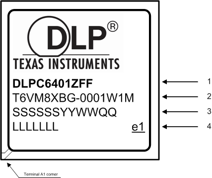
Device Marking

DLPC6401 DPP6401 datasheet package marking drawings_061615_3.png

Marking Definitions:

Line 1: DLP® device name

Line 2: Foundry part number

Line 3: SSSSSSYYWW-QQ: Package assembly information

SSSSSS: Manufacturing site

YYWW: Date code (YY = Year :: WW = Week)

QQ: Qualification level option – Engineering samples are marked in this field with a -ES suffix.

For example, TAIWAN1324-ES would be engineering samples built in Taiwan the 24th week of 2013.

Line 4: LLLLLLL e1: Manufacturing Lot Code for Semiconductor Wafers and Lead-free Solder Ball Marking

LLLLLLL: Manufacturing lot code

e1: Lead-free solder balls consisting of SnAgCu