DLPS031C December 2013 – August 2015 DLPC6401
PRODUCTION DATA.
- 1 Features
- 2 Applications
- 3 Description
- 4 Revision History
- 5 Pin Configuration and Functions
-
6 Specifications
- 6.1 Absolute Maximum Ratings
- 6.2 ESD Ratings
- 6.3 Recommended Operating Conditions
- 6.4 Thermal Information
- 6.5 Electrical Characteristics
- 6.6 Electrical Characteristics (Normal Mode)
- 6.7 System Oscillators Timing Requirements
- 6.8 Test and Reset Timing Requirements
- 6.9 JTAG Interface: I/O Boundary Scan Application Timing Requirements
- 6.10 Port 1 Input Pixel Interface Timing Requirements
- 6.11 Port 2 Input Pixel Interface (FPD-Link Compatible LVDS Input) Timing Requirements
- 6.12 Synchronous Serial Port (SSP) Interface Timing Requirements
- 6.13 Programmable Output Clocks Switching Characteristics
- 6.14 Synchronous Serial Port (SSP) Interface Switching Characteristics
- 6.15 JTAG Interface: I/O Boundary Scan Application Switching Characteristics
- 7 Detailed Description
- 8 Application and Implementation
- 9 Power Supply Recommendations
- 10Layout
- 11Device and Documentation Support
- 12Mechanical, Packaging, and Orderable Information
Package Options
Mechanical Data (Package|Pins)
- ZFF|419
Thermal pad, mechanical data (Package|Pins)
7.3.1.2 System Reset Operation
Immediately following any type of system reset (power-up reset, PWRGOOD reset, watchdog timer timeout, and so on), the DLPC6401 device automatically returns to NORMAL power mode and returns to the following state.
- All GPIO tri-state and as a result, all GPIO-controlled voltage switches default to enabling power to all ASIC supply lines. (Assume these outputs are externally pulled-high.)
- The master PLL remains active (it is reset only after a power-up reset sequence) and most of the derived clocks are active. However, only those resets associated with the ARM9 processor and its peripherals are released. (The ARM9 is responsible for releasing all other resets.)
- ARM9 associated clocks default to their full clock rates. (Boot-up is a full speed.)
- All front-end derived clocks are disabled.
- The PLL feeding the DDR DMD I/F (PLLD) defaults to its power-down mode and all derived clocks are inactive with corresponding resets asserted. (The ARM9 is responsible for enabling these clocks and releasing associated resets.)
- DMD I/O (except DMD_DAD_OEZ) defaults to its outputs in a logic low state. DMD_DAD_OEZ defaults tri-stated, but should be pulled high through an external 30- to 51-kΩ pullup resistor on the PCB.
- All resets output by the DLPC6401 device remain asserted until released by the ARM9 (after boot-up).
- The ARM9 processor boots-up from external flash.
When the ARM9 boots-up, the ARM9 API:
- Configures the programmable DDR clock generator (DCG) clock rates (that is, the DMD LPDDR I/F rate)
- Enables the DCG PLL (PLLD) while holding divider logic in reset
- When the DCG PLL locks, ARM9 software sets DMD clock rates
- API software then releases DCG divider logic resets, which in turn, enable all derived DCG clocks
- Releases external resets
Application software then typically waits for a wake-up command (through the soft power switch on the projector) from the end user. When the projector is requested to wake-up, the software places the ASIC back in normal mode, re-initialize clocks, and resets as required.

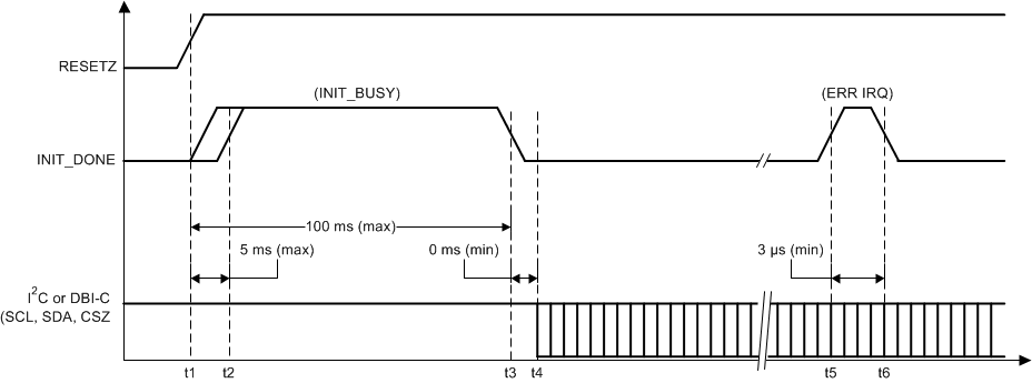
- t2: device drives INIT_DONE high within 5 ms after reset is release. Indicates auto-initialization is busy
- t3: I2C or DBI-C access to DLPC6401 device does not start until the INIT_BUSY flag (on INIT_DONE) goes low. This can occur within 100 ms, but may take several seconds
- t5: an active high pulse on INIT_DONE following the initialization period indicates a detected error condition. The device reports the source of the error in the system status.