DLPS031C December 2013 – August 2015 DLPC6401
PRODUCTION DATA.
- 1 Features
- 2 Applications
- 3 Description
- 4 Revision History
- 5 Pin Configuration and Functions
-
6 Specifications
- 6.1 Absolute Maximum Ratings
- 6.2 ESD Ratings
- 6.3 Recommended Operating Conditions
- 6.4 Thermal Information
- 6.5 Electrical Characteristics
- 6.6 Electrical Characteristics (Normal Mode)
- 6.7 System Oscillators Timing Requirements
- 6.8 Test and Reset Timing Requirements
- 6.9 JTAG Interface: I/O Boundary Scan Application Timing Requirements
- 6.10 Port 1 Input Pixel Interface Timing Requirements
- 6.11 Port 2 Input Pixel Interface (FPD-Link Compatible LVDS Input) Timing Requirements
- 6.12 Synchronous Serial Port (SSP) Interface Timing Requirements
- 6.13 Programmable Output Clocks Switching Characteristics
- 6.14 Synchronous Serial Port (SSP) Interface Switching Characteristics
- 6.15 JTAG Interface: I/O Boundary Scan Application Switching Characteristics
- 7 Detailed Description
- 8 Application and Implementation
- 9 Power Supply Recommendations
- 10Layout
- 11Device and Documentation Support
- 12Mechanical, Packaging, and Orderable Information
Package Options
Mechanical Data (Package|Pins)
- ZFF|419
Thermal pad, mechanical data (Package|Pins)
9.2 System Power-Up Sequence
Although the DLPC6401 device requires an array of power supply voltages (1.2 V, 1.8 V, 1.9 V, and 3.3 V), there are no restrictions regarding the relative order of power supply sequencing. This is true for both power-up and power-down scenarios. Similarly, there is no minimum time between powering-up and powering-down the different supplies feeding the DLPC6401 device. However, note that it is not uncommon for there to be power-sequencing requirements for the devices that share the supplies with the DLPC6401 device. For example:
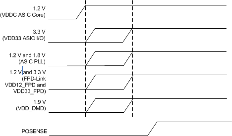
- 1.2-V core power should be applied whenever any I/O power is applied. This ensures the state of the associated I/O that are powered are controlled to a known state. Thus, TI recommends to apply core power first. Other supplies should be applied only after the 1.2-V ASIC core has ramped up.
- All ASIC power should be applied before POSENSE is asserted to ensure proper power-up initialization is performed. 1.8-V PLL power, 1.9-V I/O power, and 3.3-V I/O power should remain applied as long as 1.2-V core power is applied and POSENSE is asserted.
It is assumed that all DLPC6401 device power-up sequencing is handled by external hardware. It is also assumed that an external power monitor will hold the DLPC6401 device in system reset during power-up (that is, POSENSE = 0). It should continue to assert system reset until all ASIC voltages have reached minimum specified voltage levels. During this time, all ASIC I/O are either tri-stated or driven low. The master PLL (PLLM) is released from reset upon the low-to-high transition of POSENSE, but the DLPC6401 device keeps the rest of the ASIC in reset for an additional 100 ms to allow the PLL to lock and stabilize its outputs. After this 100-ms delay, ARM9-related internal resets are de-asserted, causing the microprocessor to begin its boot-up routine.
Figure 16 shows the recommended DLPC6401 system power-up sequence.
 Figure 16. System Power-Up Sequence