SLOSE59C May 2020 – July 2022 DRV8424 , DRV8425
PRODUCTION DATA
- 1 Features
- 2 Applications
- 3 Description
- 4 Revision History
- 5 Pin Configuration and Functions
- 6 Specifications
-
7 Detailed Description
- 7.1 Overview
- 7.2 Functional Block Diagram
- 7.3
Feature Description
- 7.3.1 Stepper Motor Driver Current Ratings
- 7.3.2 PWM Motor Drivers
- 7.3.3 Microstepping Indexer
- 7.3.4 Controlling VREF with an MCU DAC
- 7.3.5 Current Regulation
- 7.3.6
Decay Modes
- 7.3.6.1 Slow Decay for Increasing and Decreasing Current
- 7.3.6.2 Slow Decay for Increasing Current, Mixed Decay for Decreasing Current
- 7.3.6.3 Mixed Decay for Increasing and Decreasing Current
- 7.3.6.4 Smart tune Dynamic Decay
- 7.3.6.5 Smart tune Ripple Control
- 7.3.6.6 PWM OFF Time
- 7.3.6.7 Blanking time
- 7.3.7 Charge Pump
- 7.3.8 Linear Voltage Regulators
- 7.3.9 Logic Level, tri-level and quad-level Pin Diagrams
- 7.3.10 nFAULT Pin
- 7.3.11 Protection Circuits
- 7.4 Device Functional Modes
- 8 Application and Implementation
- 9 Power Supply Recommendations
- 10Layout
- 11Device and Documentation Support
- 12Mechanical, Packaging, and Orderable Information
Package Options
Mechanical Data (Package|Pins)
Thermal pad, mechanical data (Package|Pins)
- RGE|24
Orderable Information
7.3.9 Logic Level, tri-level and quad-level Pin Diagrams
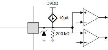
Figure 7-17 shows the input structure for M0, DECAY0, DECAY1 and ENABLE pins.
 Figure 7-17 Tri-Level Input Pin Diagram
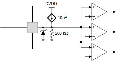
Figure 7-17 shows the input structure for M1 and TOFF pins.
 Figure 7-18 Quad-Level Input Pin Diagram
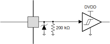
Figure 7-19 shows the input structure for STEP, DIR and nSLEEP pins.
 Figure 7-19 Logic-Level Input Pin Diagram