SLVSDX8B March 2017 – December 2018 DRV8702D-Q1 , DRV8703D-Q1
PRODUCTION DATA.
- 1 Features
- 2 Applications
- 3 Description
- 4 Revision History
- 5 Pin Configuration and Functions
- 6 Specifications
-
7 Detailed Description
- 7.1 Overview
- 7.2 Functional Block Diagram
- 7.3
Feature Description
- 7.3.1 Bridge Control
- 7.3.2 MODE Pin
- 7.3.3 nFAULT Pin
- 7.3.4 Current Regulation
- 7.3.5 Amplifier Output (SO)
- 7.3.6 PWM Motor Gate Drivers
- 7.3.7 IDRIVE Pin (DRV8702D-Q1 Only)
- 7.3.8 Dead Time
- 7.3.9 Propagation Delay
- 7.3.10 Overcurrent VDS Monitor
- 7.3.11 VDS Pin (DRV8702D-Q1 Only)
- 7.3.12 Charge Pump
- 7.3.13 Gate Drive Clamp
- 7.3.14
Protection Circuits
- 7.3.14.1 VM Undervoltage Lockout (UVLO2)
- 7.3.14.2 Logic Undervoltage (UVLO1)
- 7.3.14.3 VCP Undervoltage Lockout (CPUV)
- 7.3.14.4 Overcurrent Protection (OCP)
- 7.3.14.5 Gate Driver Fault (GDF)
- 7.3.14.6 Thermal Shutdown (TSD)
- 7.3.14.7 Watchdog Fault (WDFLT, DRV8703D-Q1 Only)
- 7.3.14.8 Reverse Supply Protection
- 7.3.15 Hardware Interface
- 7.4 Device Functional Modes
- 7.5 Programming
- 7.6 Register Maps
- 8 Application and Implementation
- 9 Power Supply Recommendations
- 10Layout
- 11Device and Documentation Support
- 12Mechanical, Packaging, and Orderable Information
Package Options
Refer to the PDF data sheet for device specific package drawings
Mechanical Data (Package|Pins)
- RHB|32
Thermal pad, mechanical data (Package|Pins)
- RHB|32
Orderable Information
6.7 Switching Characteristics
Over recommended operating conditions unless otherwise noted| PARAMETER | TEST CONDITIONS | MIN | TYP | MAX | UNIT | |
|---|---|---|---|---|---|---|
| POWER SUPPLIES (VM, AVDD, DVDD) | ||||||
| t(SLEEP) | Sleep time | nSLEEP = low to sleep mode | 100 | µs | ||
| t(wu) | Wake-up time | nSLEEP = high to output change | 1 | ms | ||
| ton | Turn on time | VM > UVLO2 to output transition | 1 | ms | ||
| CHARGE PUMP (VCP, CPH, CPL) | ||||||
| fS(VCP) | Charge-pump switching frequency | VM > UVLO2 | 200 | 400 | 700 | kHz |
| CONTROL INPUTS (IN1, IN2, nSLEEP, MODE, nSCS, SCLK, SDI, PH, EN) | ||||||
| tpd | Propagation delay | removed PH and EN pinsIN1, IN2 to GH or GL | 500 | ns | ||
| FET GATE DRIVERS (GH1, GH2, SH1, SH2, GL1, GL2) | ||||||
| t(DEAD) | Output dead time (DRV8702D-Q1) | Observed t(DEAD) depends on IDRIVE setting | 240 | ns | ||
| t(DEAD) | Output dead time (DRV8703D-Q1) | TDEAD = 2’b00; Observed t(DEAD) depends on IDRIVE setting | 120 | ns | ||
| TDEAD = 2’b01; Observed t(DEAD) depends on IDRIVE setting | 240 | |||||
| TDEAD = 2’b10; Observed t(DEAD) depends on IDRIVE setting | 480 | |||||
| TDEAD = 2’b11; Observed t(DEAD) depends on IDRIVE setting | 960 | |||||
| t(DRIVE) | Gate drive time | 2.5 | µs | |||
| CURRENT SHUNT AMPLIFIER AND PWM CURRENT CONTROL (SP, SN, SO, VREF) | ||||||
| tS | Settling time to ±1%(1) | VSP = VSN = GND to VSP = 240 mV, VSN = GND, AV= 10; C(SO) = 200 pF | 0.5 | µs | ||
| VSP = VSN = GND to VSP = 120 mV, VSN = GND, AV= 20; C(SO) = 200 pF | 1 | |||||
| VSP = VSN = GND to VSP = 60 mV, VSN = GND, AV= 40; C(SO) = 200 pF | 2 | |||||
| VSP = VSN = GND to VSP = 30 mV, VSN = GND, AV= 80; C(SO) = 200 pF | 4 | |||||
| toff | PWM off-time (DRV8702D-Q1) | 25 | µs | |||
| toff | PWM off-time (DRV8703D-Q1) | TOFF = 00 | 25 | µs | ||
| TOFF = 01 | 50 | |||||
| TOFF = 10 | 100 | |||||
| TOFF = 11 | 200 | |||||
| t(BLANK) | PWM blanking time | 2 | µs | |||
| PROTECTION CIRCUITS | ||||||
| t(UVLO) | VM UVLO falling deglitch time | VM falling; UVLO report | 10 | µs | ||
| t(OCP) | Overcurrent deglitch time | 3.7 | 4 | 4.3 | µs | |
| t(RETRY) | Overcurrent retry time | 2.8 | 3 | 3.2 | ms | |
| t(WD) | Watchdog time out (DRV8703D-Q1) | WD_DLY = 2’b00 | 10 | ms | ||
| WD_DLY = 2’b01 | 20 | |||||
| WD_DLY = 2’b10 | 50 | |||||
| WD_DLY = 2’b11 | 100 | |||||
| t(RESET) | Watchdog timer reset period | 64 | µs | |||
| SPI | ||||||
| t(SPI_READY) | SPI read after power on | VM > VUVLO1 | 5 | 10 | ms | |
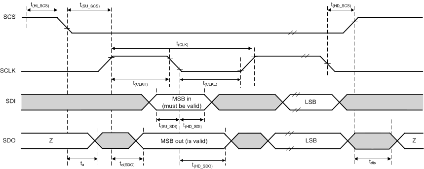
| td(SDO) | SDO output data delay time, CLK high to SDO valid | CL = 20 pF | 30 | ns | ||
| ta | SCS access time, SCS low to SDO out of high impedance | 10 | ns | |||
| tdis | SCS disable time, SCS high to SDO high impedance | 10 | ns | |||
(1) Ensured by design
 Figure 1. SPI Slave Mode Timing Definition
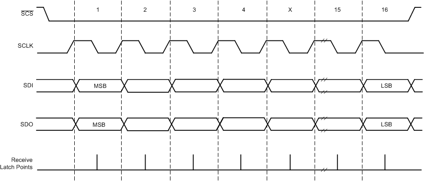
  Figure 2. SPI Slave Mode Timing Diagram