SLLSFA7A July 2020 – April 2021 DRV8706-Q1
PRODUCTION DATA
- 1 Features
- 2 Applications
- 3 Descriptions
- 4 Revision History
- 5 Pin Configuration
- 6 Specifications
-
7 Detailed Description
- 7.1 Overview
- 7.2 Functional Block Diagram
- 7.3
Feature Description
- 7.3.1 External Components
- 7.3.2 Device Interface Variants
- 7.3.3 Input PWM Modes
- 7.3.4 Smart Gate Driver
- 7.3.5 Doubler (Single-Stage) Charge Pump
- 7.3.6 Wide Common Mode Differential Current Shunt Amplifier
- 7.3.7 Pin Diagrams
- 7.3.8
Protection and Diagnostics
- 7.3.8.1 Gate Driver Disable and Enable (DRVOFF and EN_DRV)
- 7.3.8.2 Fault Reset (CLR_FLT)
- 7.3.8.3 DVDD Logic Supply Power on Reset (DVDD_POR)
- 7.3.8.4 PVDD Supply Undervoltage Monitor (PVDD_UV)
- 7.3.8.5 PVDD Supply Overvoltage Monitor (PVDD_OV)
- 7.3.8.6 VCP Charge Pump Undervoltage Lockout (VCP_UV)
- 7.3.8.7 MOSFET VDS Overcurrent Protection (VDS_OCP)
- 7.3.8.8 Gate Driver Fault (VGS_GDF)
- 7.3.8.9 Thermal Warning (OTW)
- 7.3.8.10 Thermal Shutdown (OTSD)
- 7.3.8.11 Offline Short Circuit and Open Load Detection (OOL and OSC)
- 7.3.8.12 Fault Detection and Response Summary Table
- 7.4 Device Function Modes
- 7.5 Programming
- 7.6 Register Maps
- 8 Application and Implementation
- 9 Layout
- 10Device and Documentation Support
- 11Mechanical, Packaging, and Orderable Information
Package Options
Refer to the PDF data sheet for device specific package drawings
Mechanical Data (Package|Pins)
- RHB|32
Thermal pad, mechanical data (Package|Pins)
- RHB|32
Orderable Information
7.3.8.11 Offline Short Circuit and Open Load Detection (OOL and OSC)
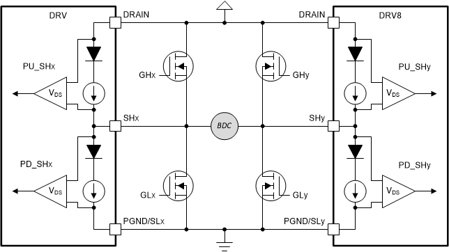
The device provides the necessary hardware to conduct offline short circuit and open load diagnostics of the external power MOSFETs and load. This is accomplished by an integrated pull up and pull down current source on the SHx pin which connect to the external half-bridge switch-node. The offline diagnostics are controlled by the associated registers bits in the OLSC_CTRL register. First, the offline diagnostic mode needs to be enabled through the OLSC_EN register setting. Then the individual current sources can be enabled through the PD_SHx and PU_SHx register settings.
The voltage on the SHx pin will be continuously monitored through the internal VDS comparators. During the diagnostic state the VDS comparators will report the real-time voltage feedback on the SHx pin node in the SPI registers in the associated VDS register status bit.
Before enabling the offline diagnostics it is recommended to place the external MOSFET half-bridges in the disabled state through the EN_DRV register setting. Additionally, the VDS comparator threshold (VDS_LVL) should be adjusted to 1-V or greater to ensure enough headroom for the internal blocking diode forward voltage drop.
On H/W device variants, this feature is not available.
To properly conduct the offline diagnostic sequence the following steps should be followed.
- Set EN_DRV control register to 0b to disable the output drivers.
- Set OLSC_EN control register to 1b to enable the offline diagnostics.
- Enable the PD_SHx and PU_SHx control registers accordingly.
- Read back the VDS_x status registers to determine output status.
- Disable the PD_SHx and PD_SHx control registers.
- Set OLSC_EN control register to 0b to disable the offline diagnostics.
- Set EN_DRV control register to 1b to enable the output drivers again.
 Figure 7-20 Offline Diagnostics