SLVSD19A June 2015 – July 2015 DRV8881
PRODUCTION DATA.
- 1 Features
- 2 Applications
- 3 Description
- 4 Revision History
- 5 Pin Configuration and Functions
- 6 Specifications
-
7 Detailed Description
- 7.1 Overview
- 7.2 Functional Block Diagrams
- 7.3
Feature Description
- 7.3.1 Motor Driver Current Ratings
- 7.3.2 PWM Motor Drivers
- 7.3.3 Bridge Control
- 7.3.4 Current Regulation
- 7.3.5 Decay Modes
- 7.3.6 Smart tune
- 7.3.7 Adaptive Blanking Time
- 7.3.8 Parallel Mode
- 7.3.9 Charge Pump
- 7.3.10 LDO Voltage Regulator
- 7.3.11 Logic and Tri-Level Pin Diagrams
- 7.3.12 Protection Circuits
- 7.4 Device Functional Modes
- 8 Application and Implementation
- 9 Power Supply Recommendations
- 10Layout
- 11Device and Documentation Support
- 12Mechanical, Packaging, and Orderable Information
Package Options
Mechanical Data (Package|Pins)
Thermal pad, mechanical data (Package|Pins)
Orderable Information
7.3.4 Current Regulation
The current through the motor windings is regulated by an adjustable fixed-off-time PWM current regulation circuit. When an H-bridge is enabled, current rises through the winding at a rate dependent on the DC voltage, inductance of the winding, and the magnitude of the back EMF present. Once the current hits the current chopping threshold, the bridge enters a decay mode for a fixed period of time to decrease the current, which is configurable between 10 and 30 µs through the tri-level input TOFF. After the off time expires, the bridge is re-enabled, starting another PWM cycle.
Table 3. Off-Time Settings
| TOFF | OFF-TIME tOFF |
|---|---|
| 0 | 20 µs |
| 1 | 30 µs |
| Z | 10 µs |
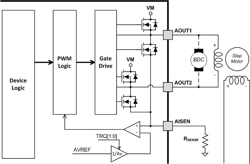
The PWM chopping current is set by a comparator which compares the voltage across a current sense resistor connected to the xISEN pin with a reference voltage. To generate the reference voltage for the current chopping comparator, the xVREF input is attenuated by a factor of Av. In addition, the TRQx pins further scale the reference.
 Figure 15. Current Regulation Block Diagram
 The chopping current is calculated as follows:

TRQ is a DAC used to scale the output current. The current scalar value for different inputs is shown in Table 4.
Table 4. Torque DAC Settings
| TRQ1 | TRQ0 | CURRENT SCALAR (TRQ) | EFFECTIVE ATTENUATION |
|---|---|---|---|
| 1 | 1 | 25% | 26.4 V/V |
| 1 | 0 | 50% | 13.2 V/V |
| 0 | 1 | 75% | 8.8 V/V |
| 0 | 0 | 100% | 6.6 V/V |