SLVSD19A June   2015  – July 2015 DRV8881

PRODUCTION DATA.  

  1. Features
  2. Applications
  3. Description
    1.     Device Images
      1.      DRV8881E Simplified System Diagram
      2.      DRV8881P Simplified System Diagram
  4. Revision History
  5. Pin Configuration and Functions
    1.     Pin Functions
    2.     DRV8881E PH/EN Pin Functions
    3.     DRV8881P PWM Pin Functions
  6. Specifications
    1. 6.1 Absolute Maximum Ratings
    2. 6.2 ESD Ratings
    3. 6.3 Recommended Operating Conditions
    4. 6.4 Thermal Information
    5. 6.5 Electrical Characteristics
    6. 6.6 Typical Characteristics
  7. Detailed Description
    1. 7.1 Overview
    2. 7.2 Functional Block Diagrams
    3. 7.3 Feature Description
      1. 7.3.1  Motor Driver Current Ratings
        1. 7.3.1.1 Peak Current Rating
        2. 7.3.1.2 RMS Current Rating
        3. 7.3.1.3 Full-Scale Current Rating
      2. 7.3.2  PWM Motor Drivers
      3. 7.3.3  Bridge Control
      4. 7.3.4  Current Regulation
      5. 7.3.5  Decay Modes
        1. 7.3.5.1 Mode 1: Slow Decay
        2. 7.3.5.2 Mode 2: Fast Decay
        3. 7.3.5.3 Mode 3: 30%/70% Mixed Decay
      6. 7.3.6  Smart tune
      7. 7.3.7  Adaptive Blanking Time
      8. 7.3.8  Parallel Mode
      9. 7.3.9  Charge Pump
      10. 7.3.10 LDO Voltage Regulator
      11. 7.3.11 Logic and Tri-Level Pin Diagrams
      12. 7.3.12 Protection Circuits
        1. 7.3.12.1 VM Undervoltage Lockout (UVLO)
        2. 7.3.12.2 VCP UVLO (CPUV)
        3. 7.3.12.3 Overcurrent Protection (OCP)
        4. 7.3.12.4 Thermal Shutdown (TSD)
    4. 7.4 Device Functional Modes
  8. Application and Implementation
    1. 8.1 Application Information
    2. 8.2 Typical Applications
      1. 8.2.1 DRV8881P Typical Application
        1. 8.2.1.1 Design Requirements
        2. 8.2.1.2 Detailed Design Procedure
          1. 8.2.1.2.1 Current Regulation
          2. 8.2.1.2.2 Stepper Motor Speed
          3. 8.2.1.2.3 Decay Modes
          4. 8.2.1.2.4 Sense Resistor
        3. 8.2.1.3 Application Curve
      2. 8.2.2 Alternate Application
        1. 8.2.2.1 Design Requirements
        2. 8.2.2.2 Detailed Design Procedure
          1. 8.2.2.2.1 Current Regulation
        3. 8.2.2.3 Application Curves
  9. Power Supply Recommendations
    1. 9.1 Bulk Capacitance Sizing
  10. 10Layout
    1. 10.1 Layout Guidelines
    2. 10.2 Layout Example
  11. 11Device and Documentation Support
    1. 11.1 Documentation Support
      1. 11.1.1 Related Documentation
    2. 11.2 Community Resources
    3. 11.3 Trademarks
    4. 11.4 Electrostatic Discharge Caution
    5. 11.5 Glossary
  12. 12Mechanical, Packaging, and Orderable Information

Package Options

Mechanical Data (Package|Pins)
Thermal pad, mechanical data (Package|Pins)
Orderable Information

Parallel Mode

To enter parallel mode on the DRV8881P, the PARA pin must be logic high during device power-up or when exiting the sleep mode. The PARA pin can be shorted to V3P3 to pull it logic high for this purpose.

In this mode, the AIN1 and AIN2 pins control the state of the outputs and the BIN1 and BIN2 pins are ignored. Similarly, the ADECAY pin controls the decay mode of the output and AVREF is used as the analog reference voltage. The BIN1, BIN2, BDECAY, and BVREF pins can be tied to GND or left Hi-Z.
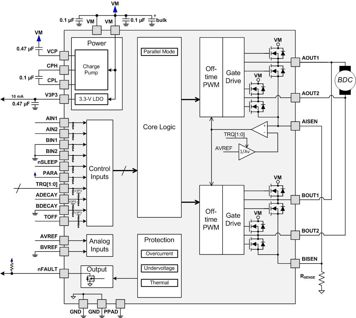
DRV8881 fbd_parallel_lvsd19.gifFigure 19. Parallel Mode Diagram