SNLS514C November 2015 – October 2019 DS280BR810
PRODUCTION DATA.
- 1 Features
- 2 Applications
- 3 Description
- 4 Revision History
- 5 Pin Configuration and Functions
- 6 Specifications
- 7 Detailed Description
- 8 Application and Implementation
- 9 Power Supply Recommendations
- 10Layout
- 11Device and Documentation Support
- 12Mechanical, Packaging, and Orderable Information
Package Options
Mechanical Data (Package|Pins)
- ZBF|135
Thermal pad, mechanical data (Package|Pins)
Orderable Information
8.2.3 Application Curves
 Figure 11. Minimal Rx/Tx Channel Test Setup
 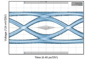 Figure 12. CAUI-4 Eye Mask with Minimal Rx/Tx Channel
 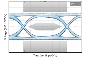 Figure 13. nPPI Eye Mask with Minimal Rx/Tx Channel
 Table 5. Settings and Measurements for CAUI-4 and nPPI with Minimal Rx/Tx Channel
| 25.78125 Gbps (CAUI-4) | 10.3125 Gbps (nPPI) | |
|---|---|---|
| DS280BR810 Rx Channel Loss | 4 dB @ 12.9 GHz | 2 dB @ 5.2 GHz |
| DS280BR810 Tx Channel Loss | 4 dB @ 12.9 GHz | 2 dB @ 5.2 GHz |
| EQ BST1 | Bypass | Bypass |
| EQ BST2 | 2 | 2 |
| EQ BW | 3 | 3 |
| VOD | 2 | 2 |
| EQ DC Gain Mode | Low | Low |
| Total Jitter @ 1E-15 | 10.4 psP-P | 10.5 psP-P |
| Differential Eye Height @ 1E-15 | 233 mVP-P | 445 mVP-P |
 Figure 14. 5 in Rx and Minimal Tx Channel Test Setup
 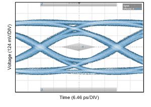 Figure 15. CAUI-4 Eye Mask with 5 in Rx and Minimal Tx Channel
 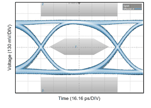 Figure 16. nPPI Eye Mask with 5 in Rx and Minimal Tx Channel
 Table 6. Settings and Measurements for CAUI-4 and nPPI with 5 in Rx and Minimal Tx Channel
| 25.78125 Gbps (CAUI-4) | 10.3125 Gbps (nPPI) | |
|---|---|---|
| Transmission Line 1 | 5 in 5 mil FR4 + 8 in SMA cable | 5 in 5 mil FR4 + 8 in SMA cable |
| DS280BR810 Rx Channel Loss | 14 dB @ 12.9 GHz | 6 dB @ 5.2 GHz |
| DS280BR810 Tx Channel Loss | 4 dB @ 12.9 GHz | 2 dB @ 5.2 GHz |
| EQ BST1 | 2 | 2 |
| EQ BST2 | 0 | 0 |
| EQ BW | 3 | 3 |
| VOD | 2 | 2 |
| EQ DC Gain Mode | Low | Low |
| Total Jitter @ 1E-15 | 11.6 psP-P | 10.4 psP-P |
| Differential Eye Height @ 1E-15 | 236 mVP-P | 504 mVP-P |
 Figure 17. 10 in Rx and Minimal Tx Channel Test Setup
 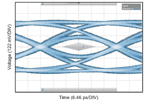 Figure 18. CAUI-4 Eye Mask with 10 in Rx and Minimal Tx Channel
 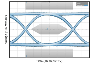 Figure 19. nPPI Eye Mask with 10 in Rx and Minimal Tx Channel
 Table 7. Settings and Measurements for CAUI-4 and nPPI with 10 in Rx and Minimal Tx Channel
| 25.78125 Gbps (CAUI-4) | 10.3125 Gbps (nPPI) | |
|---|---|---|
| Transmission Line | 10 in 5 mil FR4 + 8 in SMA cable | 10 in 5 mil FR4 + 8 in SMA cable |
| DS280BR810 Rx Channel Loss | 22 dB @ 12.9 GHz | 10 dB @ 5.2 GHz |
| DS280BR810 Tx Channel Loss | 4 dB @ 12.9 GHz | 2 dB @ 5.2 GHz |
| EQ BST1 | 4 | 4 |
| EQ BST2 | 2 | 2 |
| EQ BW | 3 | 3 |
| VOD | 2 | 2 |
| EQ DC Gain Mode | Low | Low |
| Total Jitter @ 1E-15 | 12.4 psP-P | 10.4 psP-P |
| Differential Eye Height @ 1E-15 | 148 mVP-P | 504 mVP-P |
 Figure 20. 10 in Rx and 5 in Tx Channel Test Setup
 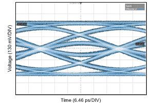 Figure 21. Linear Mode: 10 in Rx and 5 in Tx Channel
 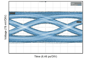 Figure 22. Limiting Mode: 10 in Rx and 5 in Tx Channel
 Table 8. Settings and Measurements for 10 in Rx and 5 in Tx Channel
| LINEAR MODE
(25.78125 Gbps) |
LIMITTING MODE
(25.78125 Gbps) |
|
|---|---|---|
| Transmission Line 1 | 10 in 5 mil FR4 + 8 in SMA cable | 10 in 5 mil FR4 + 8 in SMA cable |
| Transmission Line 2 | 5 in 5 mil FR4 + 8 in SMA cable | 5 in 5 mil FR4 + 8 in SMA cable |
| DS280BR810 Rx Channel Loss | 22 dB @ 12.9 GHz | 22 dB @ 12.9 GHz |
| DS280BR810 Tx Channel Loss | 14 dB @ 12.9 GHz | 14 dB @ 12.9 GHz |
| Total Channel Loss | 36 dB @ 12.9 GHz | 36 dB @ 12.9 GHz |
| EQ BST1 | 6 | 4 |
| EQ BST2 | 7 | 2 |
| EQ BW | 3 | 3 |
| VOD | 3 | 3 |
| EQ DC Gain Mode | Low | High |
| Tx Main-Cursor | N/A | 16 |
| Tx Pre-Cursor | N/A | -2 |
| Tx Post-Cursor | N/A | -13 |
| Total Jitter @ 1E-15 | 15.8 psP-P | 18.2 psP-P |
| Differential Eye Height @ 1E-15 | 61 mVP-P | 79 mVP-P |
 Figure 23. FIR Test Setup
 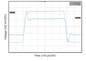 Figure 24. FIR Post-Cursor Example
 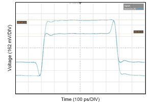 Figure 25. FIR Pre-Cursor Example
 Table 9. Example FIR Settings
| Figure 24 | Figure 25 |
|---|---|
| (Pre, Main, Post) = (0, 12, 0) | (Pre, Main, Post) = (0, 12, 0) |
| (Pre, Main, Post) = (0, 16, 15) | (Pre, Main, Post) = (11, 12, 0) |
 Figure 26. Transmit FIR Test Setup
 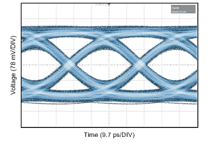 Figure 27. 25.78125 Gbps Limiting Mode with FIR
 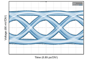 Figure 28. 28.125 Gbps Limiting Mode with FIR
 Table 10. Settings and Measurements for 5 in Tx Channel with Limiting Mode
| 25.78125 Gbps, Limiting Mode | 28.125 Gbps, Limiting Mode | |
|---|---|---|
| Transmission Line | 5 in 5 mil FR4 + 8 in SMA cable | 5 in 5 mil FR4 + 8 in SMA cable |
| DS280BR810 Tx Channel Loss | 10 dB @ 12.9 GHz | 11 dB @ 14 GHz |
| VOD | 3 | 3 |
| Main-Cursor | 16 | 15 |
| Pre-Cursor | 2 | 2 |
| Post-Cursor | 13 | 14 |
| Total Jitter @ 1E-15 | 13.8 psP-P | 15.3 psP-P |
| Differential Eye Height @ 1E-15 | 142 mVP-P | 138 mVP-P |