SNLS514C November   2015  – October 2019 DS280BR810

PRODUCTION DATA.  

  1. Features
  2. Applications
  3. Description
    1.     Simplified Schematic
  4. Revision History
  5. Pin Configuration and Functions
    1.     Pin Functions
  6. Specifications
    1. 6.1 Absolute Maximum Ratings
    2. 6.2 ESD Ratings
    3. 6.3 Recommended Operating Conditions
    4. 6.4 Thermal Information
    5. 6.5 Electrical Characteristics
    6. 6.6 Electrical Characteristics -- Serial Management Bus Interface
    7. 6.7 Timing Requirements -- Serial Management Bus Interface
    8. 6.8 Typical Characteristics
  7. Detailed Description
    1. 7.1 Overview
    2. 7.2 Functional Block Diagram
    3. 7.3 Feature Description
      1. 7.3.1 Device Data Path Operation
      2. 7.3.2 AC-Coupled Receiver and Transmitter
      3. 7.3.3 Signal Detect
      4. 7.3.4 2-Stage CTLE
      5. 7.3.5 Driver DC Gain Control
      6. 7.3.6 FIR Filter (Limiting Mode)
      7. 7.3.7 Configurable SMBus Address
    4. 7.4 Device Functional Modes
      1. 7.4.1 SMBus Slave Mode Configuration
      2. 7.4.2 SMBus Master Mode Configuration (EEPROM Self Load)
    5. 7.5 Programming
      1. 7.5.1 Transfer of Data with the SMBus Interface
    6. 7.6 Register Maps
      1. 7.6.1 Register Types: Global, Shared, and Channel
      2. 7.6.2 Global Registers: Channel Selection and ID Information
        1. Table 2. Global Register Map
      3. 7.6.3 Shared Registers
        1. Table 3. Shared Register Map
      4. 7.6.4 Channel Registers
        1. Table 4. Channel Register Map
  8. Application and Implementation
    1. 8.1 Application Information
    2. 8.2 Typical Application
      1. 8.2.1 Backplane and Mid-Plane Reach Extension
        1. 8.2.1.1 Design Requirements
        2. 8.2.1.2 Detailed Design Procedure
      2. 8.2.2 Front-Port Applications
        1. 8.2.2.1 Design Requirements
        2. 8.2.2.2 Detailed Design Procedure
      3. 8.2.3 Application Curves
    3. 8.3 Initialization Set Up
  9. Power Supply Recommendations
  10. 10Layout
    1. 10.1 Layout Guidelines
    2. 10.2 Layout Example
  11. 11Device and Documentation Support
    1. 11.1 Documentation Support
      1. 11.1.1 Related Documents
    2. 11.2 Receiving Notification of Documentation Updates
    3. 11.3 Support Resources
    4. 11.4 Trademarks
    5. 11.5 Electrostatic Discharge Caution
    6. 11.6 Glossary
  12. 12Mechanical, Packaging, and Orderable Information
    1. 12.1 Package Option Addendum
      1. 12.1.1 Packaging Information
      2. 12.1.2 Tape and Reel Information

Package Options

Mechanical Data (Package|Pins)
Thermal pad, mechanical data (Package|Pins)
Orderable Information

FIR Filter (Limiting Mode)

The DS280BR810 has an optional limiting mode with a fixed-delay 3-tap finite impulse response (FIR) filter to provide transmit equalization. This FIR can be configured to apply pre-cursor and post-cursor boost to the high speed signal. The FIR filter also allows for main cursor amplitude control. The tap polarities in the FIR filter are fixed to allow for pre-cursor or post-cursor boost to be applied to the signal.
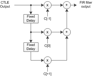
DS280BR810 FIR_Filter.gifFigure 4. 3-Tap FIR Filter Block Diagram

Linear mode is recommended for the majority of applications, especially those which require Link Training. Common protocols such as 100 GbE and 40 GbE CR4/KR4, 50 GbE and 25GbE CR, 10 GbE KR, InfiniBand EDR, and others require Link Training. Linear mode is required for Link Training so that the ASIC transmitter pre-cursor and post-cursor coefficients can propagate through the DS280BR810 in a transparent fashion. For applications which do not utilize Link Training, limiting mode may be used to provide output pre-cursor and post-cursor equalization for the purpose of improving the far-end eye opening. If the downstream receiver SerDes uses a decision feedback equalizer (DFE) to equalize the signal, the linear mode may be preferable to the limiting mode. DFE circuits often perform best when operating on a linear signal.