SNLS514C November   2015  – October 2019 DS280BR810

PRODUCTION DATA.  

  1. Features
  2. Applications
  3. Description
    1.     Simplified Schematic
  4. Revision History
  5. Pin Configuration and Functions
    1.     Pin Functions
  6. Specifications
    1. 6.1 Absolute Maximum Ratings
    2. 6.2 ESD Ratings
    3. 6.3 Recommended Operating Conditions
    4. 6.4 Thermal Information
    5. 6.5 Electrical Characteristics
    6. 6.6 Electrical Characteristics -- Serial Management Bus Interface
    7. 6.7 Timing Requirements -- Serial Management Bus Interface
    8. 6.8 Typical Characteristics
  7. Detailed Description
    1. 7.1 Overview
    2. 7.2 Functional Block Diagram
    3. 7.3 Feature Description
      1. 7.3.1 Device Data Path Operation
      2. 7.3.2 AC-Coupled Receiver and Transmitter
      3. 7.3.3 Signal Detect
      4. 7.3.4 2-Stage CTLE
      5. 7.3.5 Driver DC Gain Control
      6. 7.3.6 FIR Filter (Limiting Mode)
      7. 7.3.7 Configurable SMBus Address
    4. 7.4 Device Functional Modes
      1. 7.4.1 SMBus Slave Mode Configuration
      2. 7.4.2 SMBus Master Mode Configuration (EEPROM Self Load)
    5. 7.5 Programming
      1. 7.5.1 Transfer of Data with the SMBus Interface
    6. 7.6 Register Maps
      1. 7.6.1 Register Types: Global, Shared, and Channel
      2. 7.6.2 Global Registers: Channel Selection and ID Information
        1. Table 2. Global Register Map
      3. 7.6.3 Shared Registers
        1. Table 3. Shared Register Map
      4. 7.6.4 Channel Registers
        1. Table 4. Channel Register Map
  8. Application and Implementation
    1. 8.1 Application Information
    2. 8.2 Typical Application
      1. 8.2.1 Backplane and Mid-Plane Reach Extension
        1. 8.2.1.1 Design Requirements
        2. 8.2.1.2 Detailed Design Procedure
      2. 8.2.2 Front-Port Applications
        1. 8.2.2.1 Design Requirements
        2. 8.2.2.2 Detailed Design Procedure
      3. 8.2.3 Application Curves
    3. 8.3 Initialization Set Up
  9. Power Supply Recommendations
  10. 10Layout
    1. 10.1 Layout Guidelines
    2. 10.2 Layout Example
  11. 11Device and Documentation Support
    1. 11.1 Documentation Support
      1. 11.1.1 Related Documents
    2. 11.2 Receiving Notification of Documentation Updates
    3. 11.3 Support Resources
    4. 11.4 Trademarks
    5. 11.5 Electrostatic Discharge Caution
    6. 11.6 Glossary
  12. 12Mechanical, Packaging, and Orderable Information
    1. 12.1 Package Option Addendum
      1. 12.1.1 Packaging Information
      2. 12.1.2 Tape and Reel Information

Package Options

Mechanical Data (Package|Pins)
Thermal pad, mechanical data (Package|Pins)
Orderable Information

Layout Example

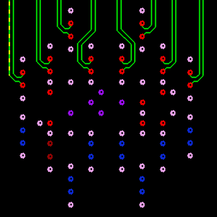
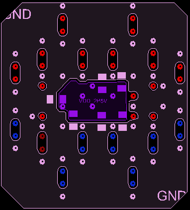
The following example layout demonstrates how all signals can be escaped from the BGA array using stripline routing on a generic 28-layer stackup. This example layout assumes the following:

  • Trace width: 0.127 mm (5 mil)
  • Trace edge-to-edge spacing: 0.152 mm (6 mil)
  • VIA finished hole size (diameter): 0.203 mm (8 mil)
  • VIA drilled hole size: 0.254 mm (10 mil)
  • VIA-to-VIA spacing: 1.0 mm (39 mil), to enhance PCB manufacturability
  • No VIA-in-pad used

Note that many other escape routing options exist using different trace width and spacing combinations. The optimum trace width and spacing will depend on the PCB material, PCB routing density, and other factors. Microstrip escape routing is also possible and may be preferable in some application scenarios, including front-port applications.
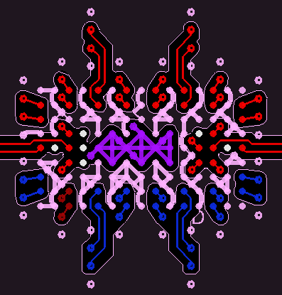
DS280BR810 top_left_top_layer_snls511.pngFigure 29. Top Layer
DS280BR810 bottom_left_internal_single_layer2_snls511.pngFigure 31. Internal Signal Layer 2
DS280BR810 top_right_internal_single_layer1_snls511.pngFigure 30. Internal Signal Layer 1
DS280BR810 bottom_layer_bottom_right_snls511.pngFigure 32. Bottom Layer