SNLS514C November 2015 – October 2019 DS280BR810
PRODUCTION DATA.
- 1 Features
- 2 Applications
- 3 Description
- 4 Revision History
- 5 Pin Configuration and Functions
- 6 Specifications
- 7 Detailed Description
- 8 Application and Implementation
- 9 Power Supply Recommendations
- 10Layout
- 11Device and Documentation Support
- 12Mechanical, Packaging, and Orderable Information
Package Options
Mechanical Data (Package|Pins)
- ZBF|135
Thermal pad, mechanical data (Package|Pins)
Orderable Information
3 Description
The DS280BR810 is an extremely low-power, high-performance eight-channel linear equalizer supporting multi-rate, multi-protocol interfaces up to 28 Gbps. It is used to extend the reach and improve the robustness of high-speed serial links for front-port, backplane, and chip-to-chip applications.
The linear nature of the DS280BR810’s equalization preserves the transmit signal characteristics, thereby allowing the host and link partner ASICs to freely negotiate transmit equalizer coefficients (100 G-CR4/KR4). This transparency to the link training protocol facilitates system-level interoperability with minimal effect on the latency. Each channel operates independently, which allows the DS280BR810 to support individual lane Forward Error Correction (FEC) pass-through.
The DS280BR810's small package dimensions, optimized high-speed signal escape, and the pin-compatible retimer portfolio make the DS280BR810 ideal for high-density backplane applications. Simplified equalization control, low power consumption, and ultra-low additive jitter make it suitable for front-port interfaces such as 100 G-SR4/LR4/CR4. The small 8-mm x 13-mm footprint easily fits behind numerous standard front-port connectors like QSFP28, SFP28, CFP2/CFP4, and CDFP without the need for a heat sink.
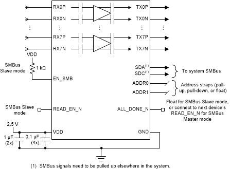
Integrated AC coupling capacitors (RX and TX) eliminate the need for external capacitors on the PCB. The DS280BR810 has a single power supply and minimal need for external components. These features reduce PCB routing complexity and bill of materials (BOM) cost.
A pin-compatible retimer device is available for longer reach applications.
The DS280BR810 can be configured either via the SMBus or through an external EEPROM. Up to 16 devices can share a single EEPROM.
Device Information (1)
| PART NUMBER | PACKAGE | BODY SIZE (NOM) |
|---|---|---|
| DS280BR810 | nFBGA (135) | 8.00 mm x 13.00 mm |
- For all available packages, see the orderable addendum at the end of the data sheet.
Simplified Schematic
