SNLS514C November   2015  – October 2019 DS280BR810

PRODUCTION DATA.  

  1. Features
  2. Applications
  3. Description
    1.     Simplified Schematic
  4. Revision History
  5. Pin Configuration and Functions
    1.     Pin Functions
  6. Specifications
    1. 6.1 Absolute Maximum Ratings
    2. 6.2 ESD Ratings
    3. 6.3 Recommended Operating Conditions
    4. 6.4 Thermal Information
    5. 6.5 Electrical Characteristics
    6. 6.6 Electrical Characteristics -- Serial Management Bus Interface
    7. 6.7 Timing Requirements -- Serial Management Bus Interface
    8. 6.8 Typical Characteristics
  7. Detailed Description
    1. 7.1 Overview
    2. 7.2 Functional Block Diagram
    3. 7.3 Feature Description
      1. 7.3.1 Device Data Path Operation
      2. 7.3.2 AC-Coupled Receiver and Transmitter
      3. 7.3.3 Signal Detect
      4. 7.3.4 2-Stage CTLE
      5. 7.3.5 Driver DC Gain Control
      6. 7.3.6 FIR Filter (Limiting Mode)
      7. 7.3.7 Configurable SMBus Address
    4. 7.4 Device Functional Modes
      1. 7.4.1 SMBus Slave Mode Configuration
      2. 7.4.2 SMBus Master Mode Configuration (EEPROM Self Load)
    5. 7.5 Programming
      1. 7.5.1 Transfer of Data with the SMBus Interface
    6. 7.6 Register Maps
      1. 7.6.1 Register Types: Global, Shared, and Channel
      2. 7.6.2 Global Registers: Channel Selection and ID Information
        1. Table 2. Global Register Map
      3. 7.6.3 Shared Registers
        1. Table 3. Shared Register Map
      4. 7.6.4 Channel Registers
        1. Table 4. Channel Register Map
  8. Application and Implementation
    1. 8.1 Application Information
    2. 8.2 Typical Application
      1. 8.2.1 Backplane and Mid-Plane Reach Extension
        1. 8.2.1.1 Design Requirements
        2. 8.2.1.2 Detailed Design Procedure
      2. 8.2.2 Front-Port Applications
        1. 8.2.2.1 Design Requirements
        2. 8.2.2.2 Detailed Design Procedure
      3. 8.2.3 Application Curves
    3. 8.3 Initialization Set Up
  9. Power Supply Recommendations
  10. 10Layout
    1. 10.1 Layout Guidelines
    2. 10.2 Layout Example
  11. 11Device and Documentation Support
    1. 11.1 Documentation Support
      1. 11.1.1 Related Documents
    2. 11.2 Receiving Notification of Documentation Updates
    3. 11.3 Support Resources
    4. 11.4 Trademarks
    5. 11.5 Electrostatic Discharge Caution
    6. 11.6 Glossary
  12. 12Mechanical, Packaging, and Orderable Information
    1. 12.1 Package Option Addendum
      1. 12.1.1 Packaging Information
      2. 12.1.2 Tape and Reel Information

Package Options

Mechanical Data (Package|Pins)
Thermal pad, mechanical data (Package|Pins)
Orderable Information

Backplane and Mid-Plane Reach Extension

The DS280BR810 has strong equalization capabilities that allow it to equalize insertion loss and extend the reach of backplane channels by 15-20 dB beyond the normal capabilities of the ASICs operating over the channel. The DS280BR810 is designed to apply gain in a linear fashion. In most cases, the DS280BR810 should be placed with the higher loss channel segment at the input and the lower loss channel segment at the output (as shown in Figure 7); however, since the DS280BR810 operates in a linear fashion, it can also be used in applications where the lower loss channel segment is at the input and the higher loss channel segment is at the output (as shown in Figure 7).
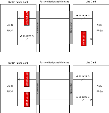
DS280BR810 BackPlaneBD.gifFigure 7. Typical Backplane and Mid-Plane Application Diagram
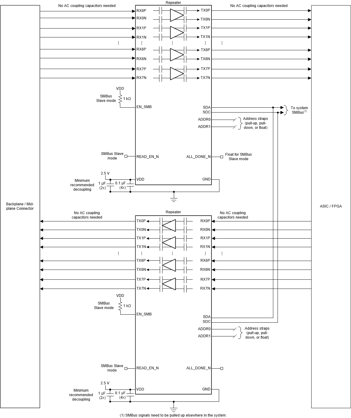
DS280BR810 BackplaneApplication.gifFigure 8. Typical Backplane and Mid-Plane Schematic