SLLSES1D December 2015 – September 2020 HD3SS3220
PRODUCTION DATA
- 1 Features
- 2 Applications
- 3 Description
- 4 Revision History
- 5 Pin Configuration and Functions
- 6 Specifications
-
7 Detailed Description
- 7.1 Overview
- 7.2 Functional Block Diagram
- 7.3
Feature Description
- 7.3.1 DFP/Source – Downstream Facing Port
- 7.3.2 UFP/Sink – Upstream Facing Port
- 7.3.3 DRP – Dual Role Port
- 7.3.4 Cable Orientation and Mux Control
- 7.3.5 Type-C Current Mode
- 7.3.6 Accessory Support
- 7.3.7 Audio Accessory
- 7.3.8 Debug Accessory
- 7.3.9 VCONN support for Active Cables
- 7.3.10 I2C and GPIO Control
- 7.3.11 HD3SS3220 V(BUS) Detection
- 7.3.12 VDD5 and VCC33 Power-On Requirements
- 7.4 Device Functional Modes
- 7.5 Programming
- 7.6
Register Maps
- 7.6.1 Device Identification Register (offset = 0x07 through 0x00) [reset = 0x00, 0x54, 0x55, 0x53, 0x42, 0x33, 0x32, 0x32]
- 7.6.2 Connection Status Register (offset = 0x08) [reset = 0x00]
- 7.6.3 Connection Status and Control Register (offset = 0x09) [reset = 0x20]
- 7.6.4 General Control Register (offset = 0x0A) [reset = 0x00]
- 7.6.5 Device Revision Register (offset = 0xA0) [reset = 0x02]
- 8 Application and Implementation
-
9 Layout
- 9.1
Layout Guidelines
- 9.1.1 Suggested PCB Stackups
- 9.1.2 High-Speed Signal Trace Length Matching
- 9.1.3 Differential Signal Spacing
- 9.1.4 High-Speed Differential Signal Rules
- 9.1.5 Symmetry in the Differential Pairs
- 9.1.6 Via Discontinuity Mitigation
- 9.1.7 Surface-Mount Device Pad Discontinuity Mitigation
- 9.1.8 ESD/EMI Considerations
- 9.2 Layout
- 9.1
Layout Guidelines
- 10Device and Documentation Support
- 11Mechanical, Packaging, and Orderable Information
Package Options
Mechanical Data (Package|Pins)
- RNH|30
Thermal pad, mechanical data (Package|Pins)
Orderable Information
3 Description
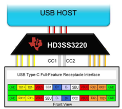
HD3SS3220 is a USB SuperSpeed (SS) 2:1 mux with DRP port controller. The device provides Channel Configuration (CC) logic and 5V VCONN sourcing for ecosystems implementing USB Type-C. The HD3SS3220 can be configured as a Downstream Facing Port (DFP), Upstream Facing Port (UFP) or a Dual Role Port (DRP) making it ideal for any application.
The HD3SS3220, in DRP mode, alternates presenting itself as a DFP or UFP according to the Type-C specifications. The CC logic block monitors the CC1 and CC2 pins for pull-up or pull-down resistances to determine when a USB port has been attached and its port role. Once a USB port has been attached, the CC logic also determines the orientation of the cable and configures the USB SS mux accordingly. Finally, CC logic advertises or detects Type-C current mode – Default, Mid, or High in DFP and UFP modes respectively.
Excellent dynamic characteristics of the integrated mux allow switching with minimum attenuation to the SS signal eye diagram and very little added jitter. The device’s switch paths deploy adaptive common mode voltage tracking resulting identical channel despite different common mode voltage for RX and TX channels.
| PART NUMBER | PACKAGE | BODY SIZE (NOM) |
|---|---|---|
| HD3SS3220 | VQFN RNH (30) | 2.50 mm x 4.50 mm |
| HD3SS3220I |
 Simplified Schematic
 Typical Application