SBOS062C September 2000 – January 2022 INA126 , INA2126
PRODUCTION DATA
- 1 Features
- 2 Applications
- 3 Description
- 4 Revision History
- 5 Pin Configuration and Functions
- 6 Specifications
- 7 Detailed Description
- 8 Application and Implementation
- 9 Power Supply Recommendations
- 10Layout
- 11Device and Documentation Support
- 12Mechanical, Packaging, and Orderable Information
Package Options
Mechanical Data (Package|Pins)
Thermal pad, mechanical data (Package|Pins)
- D|8
Orderable Information
3 Description
The INA126 and INA2126 (INAx126) are precision instrumentation amplifiers for accurate, low-noise, differential-signal acquisition. The two-op-amp design provides excellent performance with low quiescent current (175 μA/channel). These features combined with a wide operating voltage range of ±1.35 V to ±18 V make the INAx126 a great choice for portable instrumentation and data acquisition systems.
Gain can be set from 5 V/V to 10000 V/V with a single external resistor. Precision input circuitry provides low offset voltage (250 μV, maximum), low offset voltage drift (3 μV/°C, maximum), and excellent common-mode rejection.
All versions are specified for the –40°C to +85°C industrial temperature range.
| PART NUMBER | PACKAGE(1) | BODY SIZE (NOM) |
|---|---|---|
| INA126 | PDIP (8) | 6.35 mm × 9.81 mm |
| SOIC (8) | 3.91 mm × 4.90 mm | |
| VSSOP (8) | 3.00 mm × 3.00 mm | |
| INA2126 | PDIP (16) | 6.35 mm × 19.30 mm |
| SOIC (16) | 3.91 mm × 9.90 mm | |
| SSOP (16) | 3.90 mm × 4.90 mm |
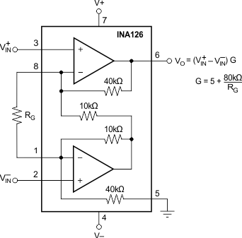
 Simplified Schematic:
INA126
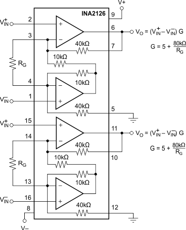
 Simplified Schematic:
INA2126