SBOS062C September   2000  – January 2022 INA126 , INA2126

PRODUCTION DATA  

  1. Features
  2. Applications
  3. Description
  4. Revision History
  5. Pin Configuration and Functions
  6. Specifications
    1. 6.1 Absolute Maximum Ratings
    2. 6.2 ESD Ratings
    3. 6.3 Recommended Operating Conditions
    4. 6.4 Thermal Information: INA126
    5. 6.5 Thermal Information: INA2126
    6. 6.6 Electrical Characteristics
    7. 6.7 Typical Characteristics
  7. Detailed Description
    1. 7.1 Overview
    2. 7.2 Functional Block Diagram
    3. 7.3 Feature Description
    4. 7.4 Device Functional Modes
      1. 7.4.1 Single-Supply Operation
  8. Application and Implementation
    1. 8.1 Application Information
    2. 8.2 Typical Application
      1. 8.2.1 Design Requirements
      2. 8.2.2 Detailed Design Procedure
        1. 8.2.2.1 Setting the Gain
        2. 8.2.2.2 Offset Trimming
        3. 8.2.2.3 Input Bias Current Return
        4. 8.2.2.4 Input Common-Mode Range
        5. 8.2.2.5 Input Protection
        6. 8.2.2.6 Channel Crosstalk—Dual Version
      3. 8.2.3 Application Curves
  9. Power Supply Recommendations
    1. 9.1 Low-Voltage Operation
  10. 10Layout
    1. 10.1 Layout Guidelines
    2. 10.2 Layout Example
  11. 11Device and Documentation Support
    1. 11.1 Device Support
      1. 11.1.1 Development Support
        1. 11.1.1.1 PSpice® for TI
    2. 11.2 Receiving Notification of Documentation Updates
    3. 11.3 Support Resources
    4. 11.4 Trademarks
    5. 11.5 Electrostatic Discharge Caution
    6. 11.6 Glossary
  12. 12Mechanical, Packaging, and Orderable Information

Package Options

Mechanical Data (Package|Pins)
Thermal pad, mechanical data (Package|Pins)
Orderable Information

Typical Characteristics

at TA = 25°C, VS = ±15 V (unless otherwise noted)

GUID-6508F047-AFEA-47EF-AFAD-68AA6B050C99-low.gif
 
Figure 6-1 Gain vs Frequency
GUID-ADF7D22B-5202-4EA2-8226-E8E372BF4837-low.gif
 
Figure 6-3 Positive Power Supply Rejection vs Frequency
GUID-A23525E6-A2B4-4445-AA87-2134A99265BC-low.gif
 VS = ±15 V
Figure 6-5 Input Common-Mode Voltage Range
vs Output Voltage
 
Figure 6-7 Input-Referred Noise vs Frequency
GUID-E9308A56-0BEB-45C3-9E54-612C75581400-low.gif
 
Figure 6-9 Input-Referred Offset Voltage WarmUp
 
Figure 6-11 Slew Rate vs Temperature
 
Figure 6-13 Output Voltage Swing vs Output Current
G = 100
Figure 6-15 Small-Signal Response
 
Figure 6-17 0.1-Hz to 10-Hz Voltage Noise
GUID-6E622E6E-570E-476D-AE10-D54C6A587F9D-low.gif
 
Figure 6-2 Common-Mode Rejection vs Frequency
GUID-C56DBC72-CE10-4622-B089-3404570B5527-low.gif
 
Figure 6-4 Negative Power Supply Rejection vs Frequency
GUID-2A028CED-C79A-484C-8D7B-C1912898DE46-low.gif
VS = ±5 V
Figure 6-6 Input Common-Mode Voltage Range
vs Output Voltage
GUID-0D4F0CE4-08BC-47DC-AF2C-ACE10BCEECF0-low.gif
 
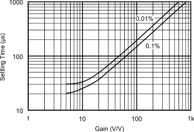
Figure 6-8 Settling Time vs Gain
 
Figure 6-10 Quiescent Current vs Temperature
GUID-3469617F-92FC-453B-8332-0DAAE9C6AED9-low.gif
 
Figure 6-12 Total Harmonic Distortion + Noise vs Frequency
G = 5
Figure 6-14 Small-Signal Response
G = 5
Figure 6-16 Large-Signal Response
GUID-2F31093B-36AA-46F6-82C8-8C6F2FE11929-low.gif
 
Figure 6-18 Channel Separation vs Frequency, RTI (Dual Version)