SLLSFJ6G December 2019 – February 2023 ISO6740 , ISO6741 , ISO6742
PRODUCTION DATA
- 1 Features
- 2 Applications
- 3 Description
- 4 Revision History
- 5 Description Continued
- 6 Pin Configuration and Functions
-
7 Specifications
- 7.1 Absolute Maximum Ratings
- 7.2 ESD Ratings
- 7.3 Recommended Operating Conditions
- 7.4 Thermal Information
- 7.5 Power Ratings
- 7.6 Insulation Specifications
- 7.7 Safety-Related Certifications
- 7.8 Safety Limiting Values
- 7.9 Electrical Characteristics—5-V Supply
- 7.10 Supply Current Characteristics—5-V Supply
- 7.11 Electrical Characteristics—3.3-V Supply
- 7.12 Supply Current Characteristics—3.3-V Supply
- 7.13 Electrical Characteristics—2.5-V Supply
- 7.14 Supply Current Characteristics—2.5-V Supply
- 7.15 Electrical Characteristics—1.8-V Supply
- 7.16 Supply Current Characteristics—1.8-V Supply
- 7.17 Switching Characteristics—5-V Supply
- 7.18 Switching Characteristics—3.3-V Supply
- 7.19 Switching Characteristics—2.5-V Supply
- 7.20 Switching Characteristics—1.8-V Supply
- 7.21 Insulation Characteristics Curves
- 7.22 Typical Characteristics
- 8 Parameter Measurement Information
- 9 Detailed Description
- 10Application and Implementation
- 11Power Supply Recommendations
- 12Layout
- 13Device and Documentation Support
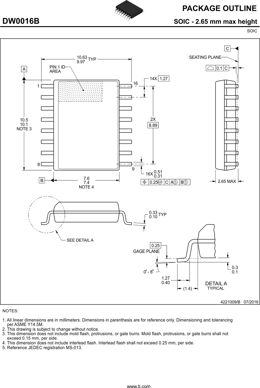
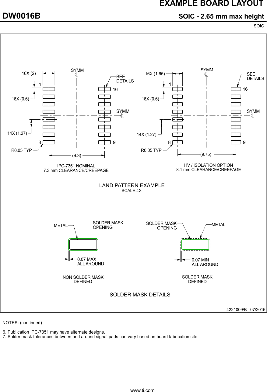
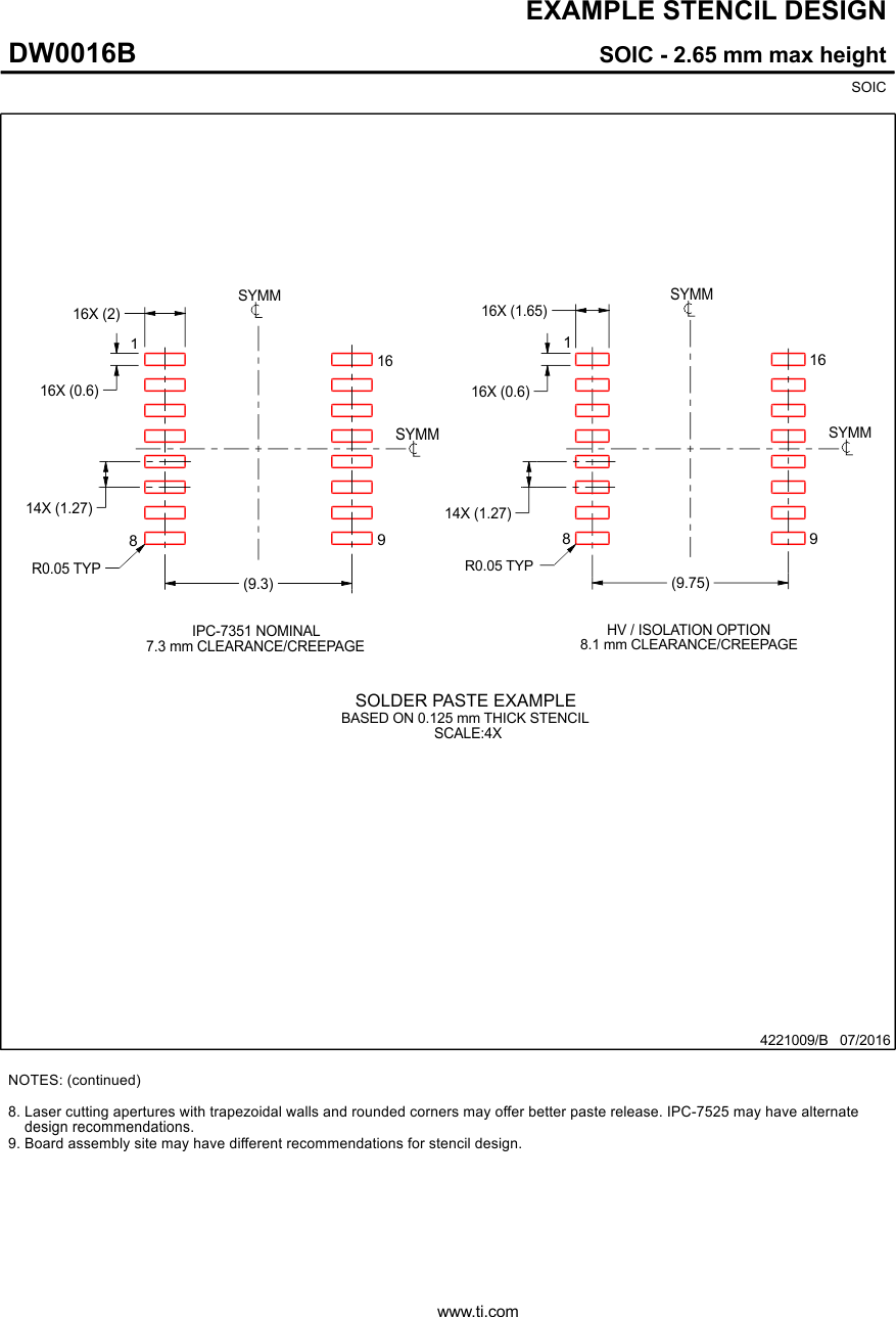
- 14Mechanical, Packaging, and Orderable Information
14.2 Tape and Reel Information
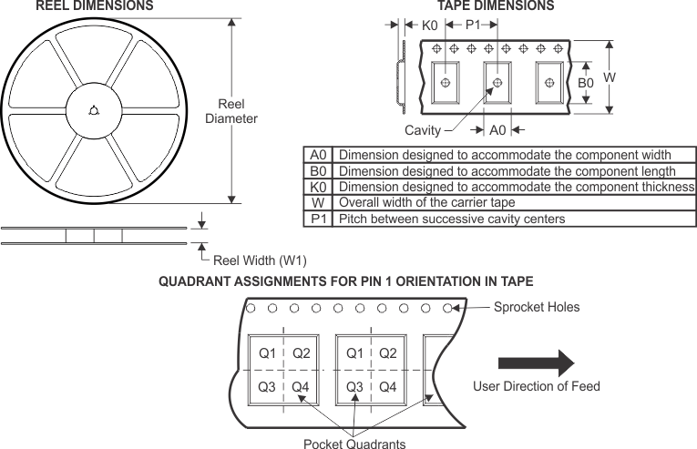
| Device | Package Type |
Package Drawing | Pins | SPQ | Reel Diameter (mm) |
Reel Width W1 (mm) |
A0 (mm) |
B0 (mm) |
K0 (mm) |
P1 (mm) |
W (mm) |
Pin1 Quadrant |
|---|---|---|---|---|---|---|---|---|---|---|---|---|
| ISO6740DWR | SOIC | DW | 16 | 2000 | 330.0 | 24.4 | 10.9 | 10.7 | 2.7 | 12.0 | 24.0 | Q1 |
| ISO6740FDWR | SOIC | DW | 16 | 2000 | 330.0 | 24.4 | 10.9 | 10.7 | 2.7 | 12.0 | 24.0 | Q1 |
| ISO6741DWR | SOIC | DW | 16 | 2000 | 330.0 | 24.4 | 10.9 | 10.7 | 2.7 | 12.0 | 24.0 | Q1 |
| ISO6741FDWR | SOIC | DW | 16 | 2000 | 330.0 | 24.4 | 10.9 | 10.7 | 2.7 | 12.0 | 24.0 | Q1 |
| ISO6742DWR | SOIC | DW | 16 | 2000 | 330.0 | 24.4 | 10.9 | 10.7 | 2.7 | 12.0 | 24.0 | Q1 |
| ISO6742FDWR | SOIC | DW | 16 | 2000 | 330.0 | 24.4 | 10.9 | 10.7 | 2.7 | 12.0 | 24.0 | Q1 |
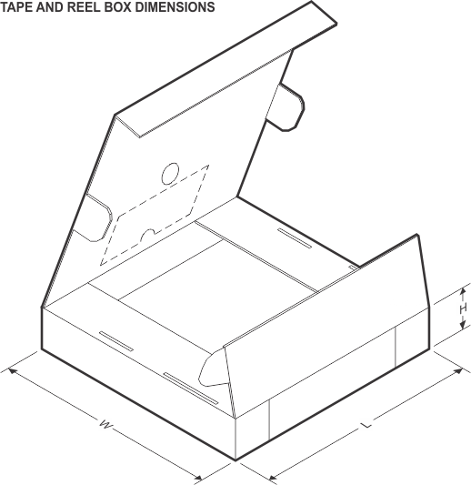
| Device | Package Type | Package Drawing | Pins | SPQ | Length (mm) | Width (mm) | Height (mm) |
|---|---|---|---|---|---|---|---|
| ISO6740DWR | SOIC | DW | 16 | 2000 | 367.0 | 367.0 | 45.0 |
| ISO6740FDWR | SOIC | DW | 16 | 2000 | 367.0 | 367.0 | 45.0 |
| ISO6741DWR | SOIC | DW | 16 | 2000 | 367.0 | 367.0 | 45.0 |
| ISO6741FDWR | SOIC | DW | 16 | 2000 | 367.0 | 367.0 | 45.0 |
| ISO6742DWR | SOIC | DW | 16 | 2000 | 367.0 | 367.0 | 45.0 |
| ISO6742FDWR | SOIC | DW | 16 | 2000 | 367.0 | 367.0 | 45.0 |