SWRS283A June 2022 – November 2022 IWR6243
PRODUCTION DATA
- 1 Features
- 2 Applications
- 3 Description
- 4 Functional Block Diagram
- 5 Revision History
- 6 Device Comparison
- 7 Terminal Configuration and Functions
-
8 Specifications
- 8.1 Absolute Maximum Ratings
- 8.2 ESD Ratings
- 8.3 Power-On Hours (POH)
- 8.4 Recommended Operating Conditions
- 8.5 Power Supply Specifications
- 8.6 Power Consumption Summary
- 8.7 RF Specification
- 8.8 Thermal Resistance Characteristics for FCBGA Package [ABL0161]
- 8.9
Timing and Switching Characteristics
- 8.9.1 Power Supply Sequencing and Reset Timing
- 8.9.2 Synchronized Frame Triggering
- 8.9.3 Input Clocks and Oscillators
- 8.9.4 Multibuffered / Standard Serial Peripheral Interface (MibSPI)
- 8.9.5 Inter-Integrated Circuit Interface (I2C)
- 8.9.6 LVDS Interface Configuration
- 8.9.7 General-Purpose Input/Output
- 8.9.8 Camera Serial Interface (CSI2)
- 9 Detailed Description
- 10Monitoring and Diagnostic Mechanisms
- 11Applications, Implementation, and Layout
- 12Device and Documentation Support
- 13Mechanical, Packaging, and Orderable Information
Package Options
Refer to the PDF data sheet for device specific package drawings
Mechanical Data (Package|Pins)
- ABL|161
Thermal pad, mechanical data (Package|Pins)
Orderable Information
8.9.3.1 Clock Specifications
An external crystal is connected to the device pins. #FIG_D1E247917 shows the crystal implementation.
 Figure 8-4 Crystal Implementation
The load capacitors, Cf1 and Cf2 in #FIG_D1E247917, should be chosen such that #T4362547-51 is satisfied. CL in the equation is the load specified by the crystal manufacturer. All discrete components used to implement the oscillator circuit should be placed as close as possible to the associated oscillator CLKP and CLKM pins.Note that Cf1 and Cf2 include the parasitic capacitances due to PCB routing.
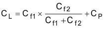
Table 8-6 lists the electrical characteristics of the clock crystal.
| NAME | DESCRIPTION | MIN | TYP | MAX | UNIT |
|---|---|---|---|---|---|
| fP | Parallel resonance crystal frequency | 40 | MHz | ||
| CL | Crystal load capacitance | 5 | 8 | 12 | pF |
| ESR | Crystal ESR | 50 | Ω | ||
| Temperature range | Expected temperature range of operation | –40 | 125 | °C | |
| Frequency tolerance | Crystal frequency tolerance#T4362547-60#T4362547-61 | -200 | 200 | ppm | |
| Drive level | 50 | 200 | µW |
In the case where an external clock is used as the clock resource, the signal is fed to the CLKP pin only; CLKM is grounded. The phase noise requirement is very important when a 40-MHz clock is fed externally. Table 8-7 lists the electrical characteristics of the external clock signal.
| PARAMETER | SPECIFICATION | UNIT | |||
|---|---|---|---|---|---|
| MIN | TYP | MAX | |||
| Input Clock: External AC-coupled sine wave or DC-coupled square wave Phase Noise referred to 40 MHz | Frequency | 40 | MHz | ||
| AC-Amplitude | 700 | 1200 | mV (pp) | ||
| DC-trise/fall | 10 | ns | |||
| Phase Noise at 1 kHz | –132 | dBc/Hz | |||
| Phase Noise at 10 kHz | –143 | dBc/Hz | |||
| Phase Noise at 100 kHz | –152 | dBc/Hz | |||
| Phase Noise at 1 MHz | –153 | dBc/Hz | |||
| Duty Cycle | 35 | 65 | % | ||
| Freq Tolerance | –50 | 50 | ppm | ||
| Input clock requirements for Secondary device in cascade mode (assuming the 20Ghz clock is provided from the Primary device in cascade) | Phase Noise at 10 kHz | -127 | dBc/Hz | ||
| Phase Noise at 100 kHz | -137 | dBc/Hz | |||
| Phase Noise at 1 MHz | -147 | dBc/Hz | |||
| Period jitter @40Mhz | 1.75 | ps rms | |||
| Spur levels (sum of all spurs) | -52 | dBc | |||