SNOS412Q February 2000 – January 2023 LM1117
PRODUCTION DATA
- 1 Features
- 2 Applications
- 3 Description
- 4 Revision History
- 5 Device Comparison Table
- 6 Pin Configuration and Functions
- 7 Specifications
- 8 Detailed Description
- 9 Application and Implementation
- 10Device and Documentation Support
- 11Mechanical, Packaging, and Orderable Information
Package Options
Mechanical Data (Package|Pins)
Thermal pad, mechanical data (Package|Pins)
- KTT|3
Orderable Information
9.5.1.1 Heat Sink Requirements
When an integrated circuit operates with an appreciable current, the junction temperature is elevated. The thermal limits must be quantified in order to achieve acceptable performance and reliability. This limit is determined by summing the individual parts consisting of a series of temperature rises from the semiconductor junction to the operating environment. A one-dimensional steady-state model of conduction heat transfer is demonstrated in Figure 9-9. The heat generated at the device junction flows through the die to the die attach pad, through the lead frame to the surrounding case material, to the printed circuit board, and eventually to the ambient environment. Below is a list of variables that may affect the thermal resistance and in turn the need for a heat sink.
| RθJC (COMPONENT VARIABLES) | RθJA (Application Variables) |
|---|---|
| Lead frame size and material | Mounting pad size, material, and location |
| No. of conduction pins | Placement of mounting pad |
| Die size | PCB size and material |
| Die attach material | Traces length and width |
| Molding compound size and material | Adjacent heat sources |
| Volume of air | |
| Ambient temperature | |
| Shape of mounting pad |

The LM1117 regulators have internal thermal shutdown to protect the device from over-heating. Under all possible operating conditions, the junction temperature of the LM1117 must be within the range of 0°C to +125°C. A heat sink can be required depending on the maximum power dissipation and maximum ambient temperature of the application. To determine if a heat sink is needed, the power dissipated by the regulator, PD , must be calculated:
Figure 9-10 shows the voltages and currents which are present in the circuit.
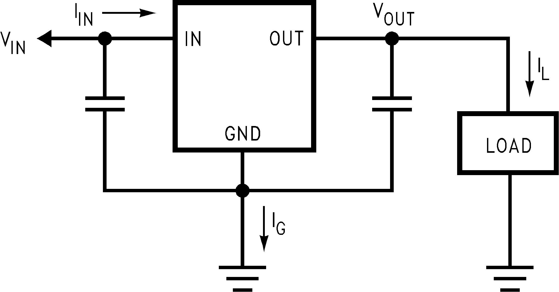 Figure 9-10 Power Dissipation Diagram
The next parameter which must be calculated is the maximum allowable temperature rise, TR(max):
where
- TJ(max) is the maximum allowable junction temperature (125°C) which is encountered in the application
- TA(max) is the maximum ambient temperature which is encountered in the application
Using the calculated values for TR(max) and PD, the maximum allowable value for the junction-to-ambient thermal resistance (RθJA) can be calculated:
For the maximum allowable value for θJA, see the Section 7.4 table.
As a design aid, Table 9-2 shows the value of the θJA of SOT-223 and TO-252 for different heat sink area. Figure 9-11 and Figure 9-12 reflects the same test results as what are in the Table 9-2
Figure 9-13 and Figure 9-14 shows the maximum allowable power dissipation vs. ambient temperature for the SOT-223 and TO-252 device. Figure 9-15 and Figure 9-16 shows the maximum allowable power dissipation vs. copper area (in2) for the SOT-223 and TO-252 devices. Please see AN1028 for power enhancement techniques to be used with SOT-223 and TO-252 packages.
The AN-1187 Leadless Leadframe Package (LLP) application note discusses improved thermal performance and power dissipation for the WSON.
| LAYOUT | COPPER AREA | THERMAL RESISTANCE | ||
|---|---|---|---|---|
| Top Side (in2)(1) | Bottom Side (in2) | (θJA,°C/W) SOT-223 | (θJA,°C/W) TO-252 | |
| 1 | 0.0123 | 0 | 136 | 103 |
| 2 | 0.066 | 0 | 123 | 87 |
| 3 | 0.3 | 0 | 84 | 60 |
| 4 | 0.53 | 0 | 75 | 54 |
| 5 | 0.76 | 0 | 69 | 52 |
| 6 | 1 | 0 | 66 | 47 |
| 7 | 0 | 0.2 | 115 | 84 |
| 8 | 0 | 0.4 | 98 | 70 |
| 9 | 0 | 0.6 | 89 | 63 |
| 10 | 0 | 0.8 | 82 | 57 |
| 11 | 0 | 1 | 79 | 57 |
| 12 | 0.066 | 0.066 | 125 | 89 |
| 13 | 0.175 | 0.175 | 93 | 72 |
| 14 | 0.284 | 0.284 | 83 | 61 |
| 15 | 0.392 | 0.392 | 75 | 55 |
| 16 | 0.5 | 0.5 | 70 | 53 |
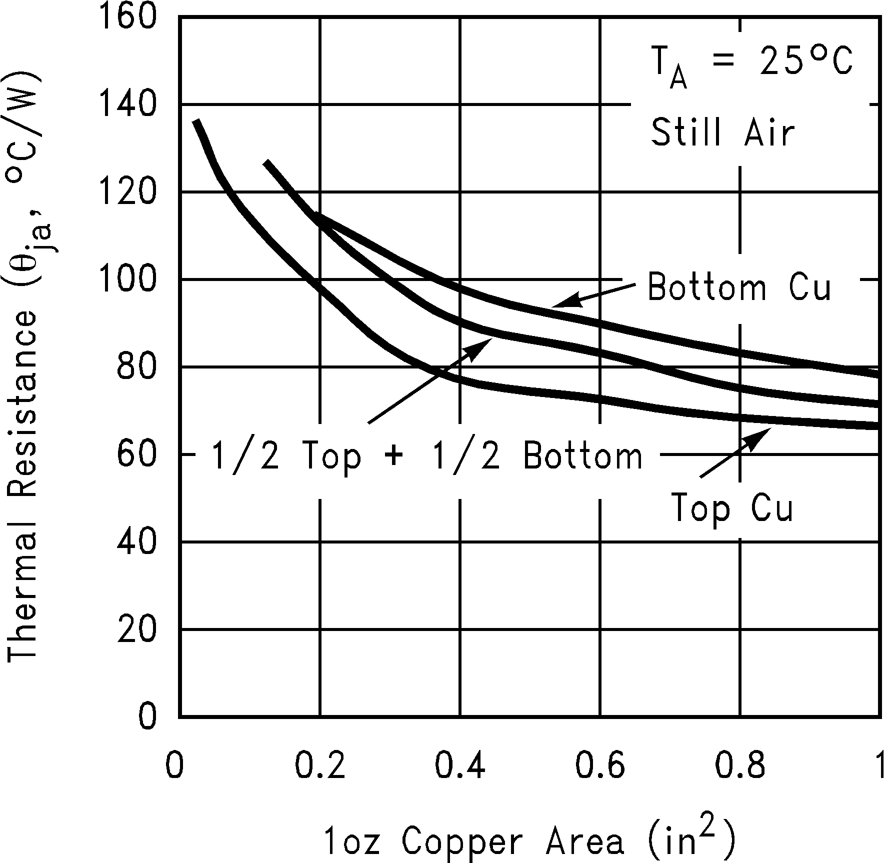 Figure 9-11 RθJA vs 1-oz Copper Area for SOT-223
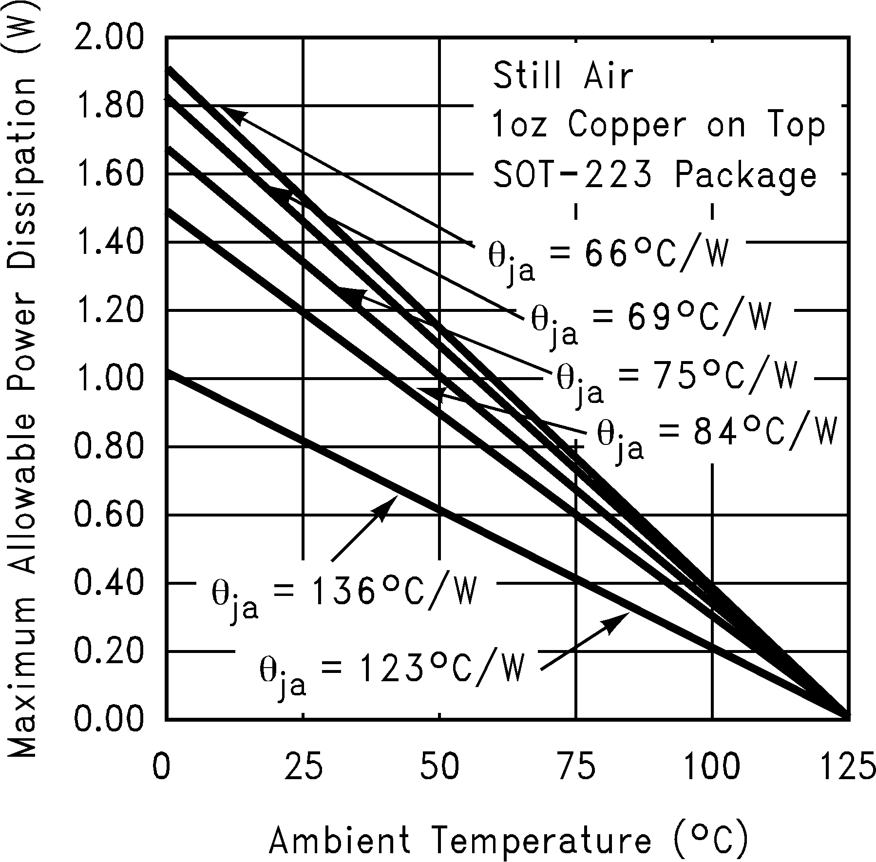 Figure 9-13 Maximum Allowable Power Dissipation vs Ambient Temperature for SOT-223
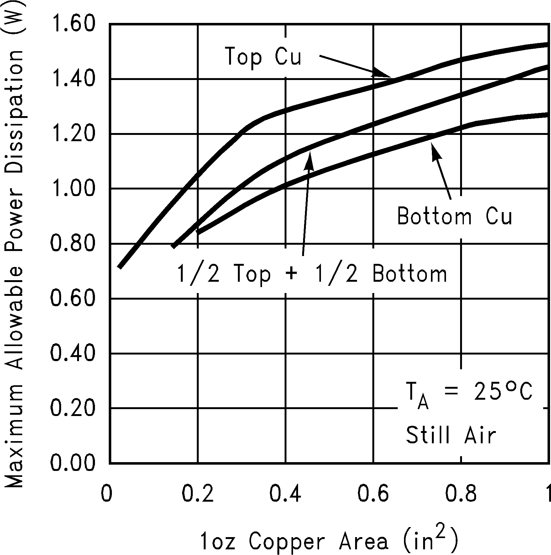 Figure 9-15 Maximum Allowable Power Dissipation vs 1-oz Copper Area for SOT-223
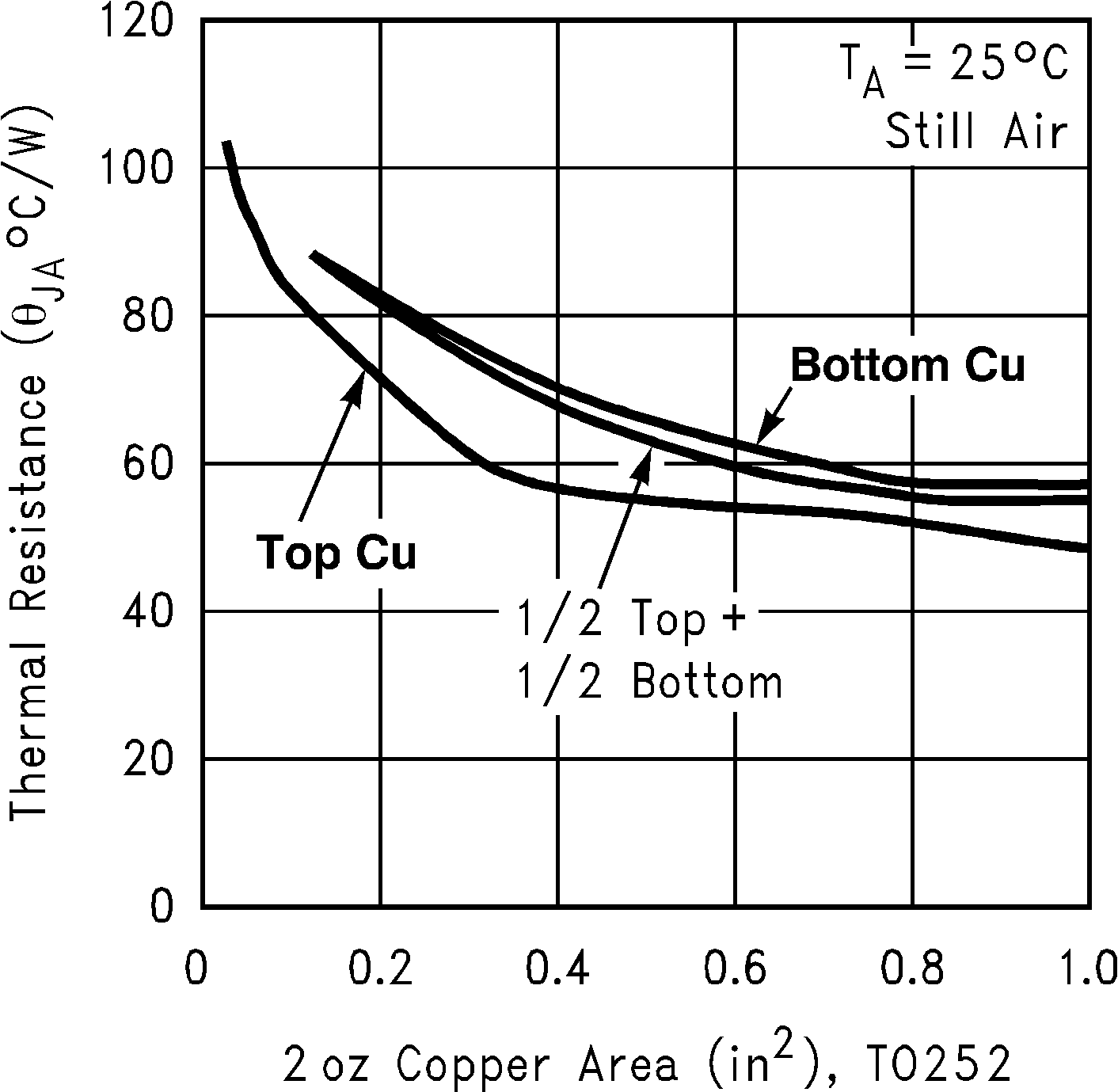 Figure 9-12 RθJA vs 2-oz Copper Area for TO-252
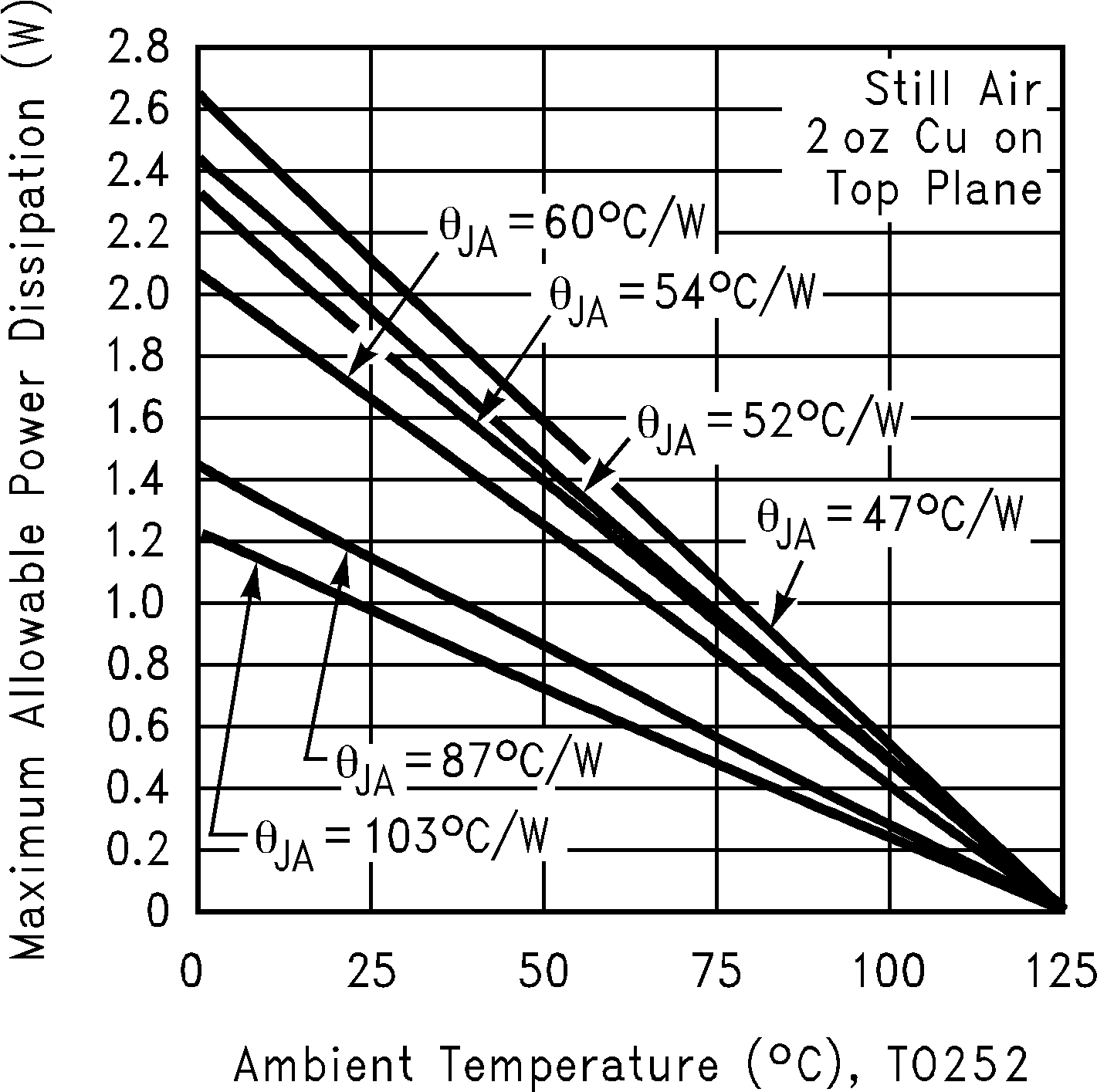 Figure 9-14 Maximum Allowable Power Dissipation vs Ambient Temperature for TO-252
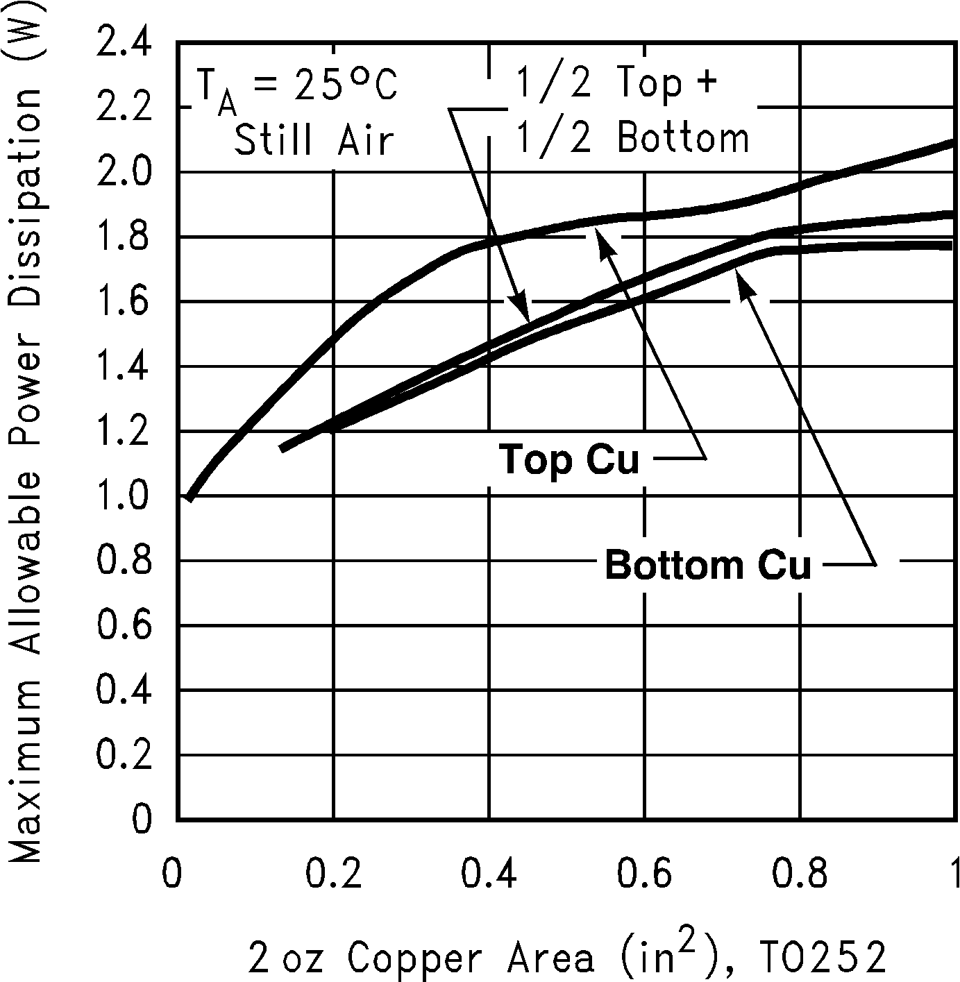 Figure 9-16 Maximum Allowable Power Dissipation vs 2-oz Copper Area for TO-252
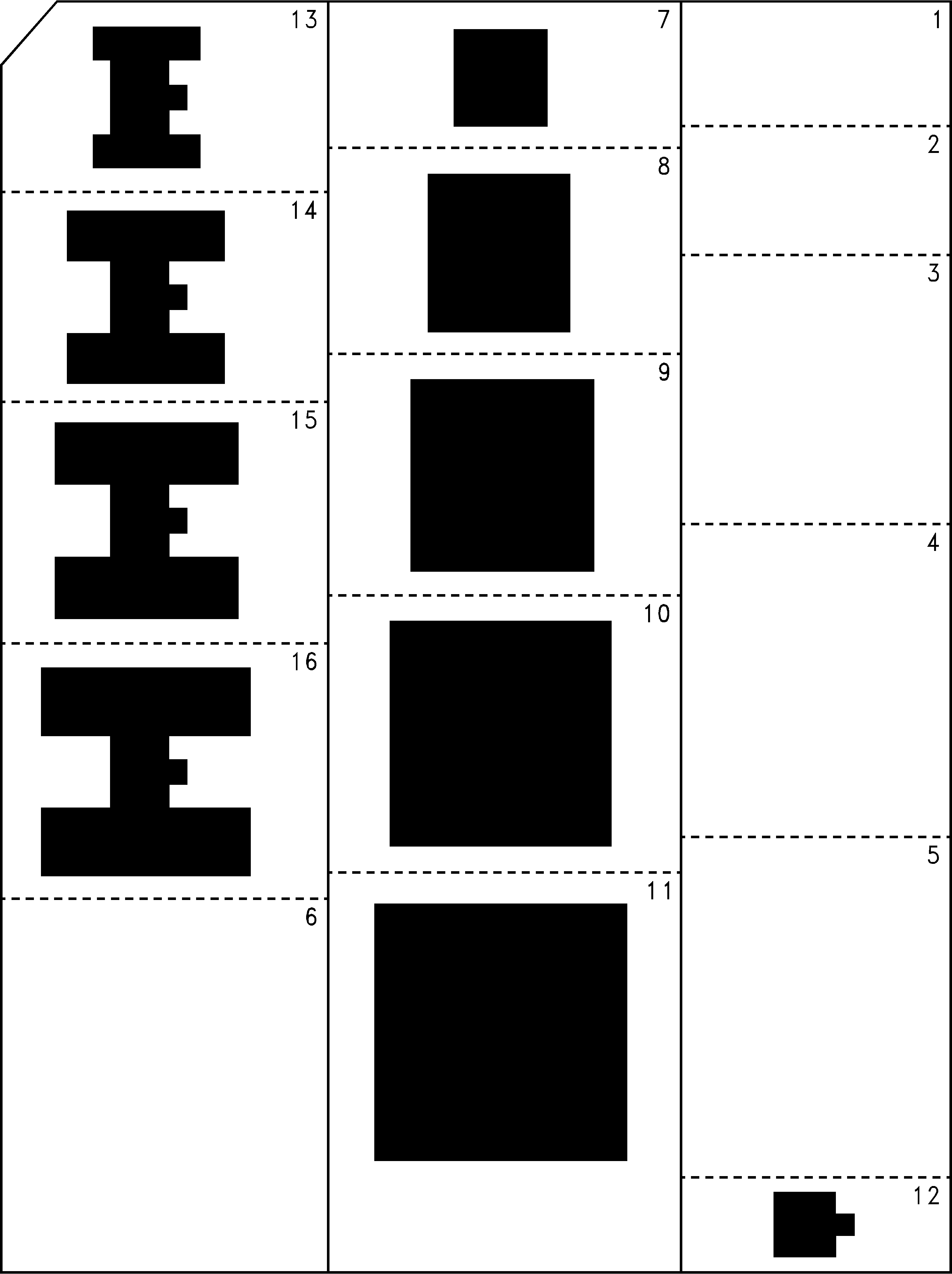 Figure 9-17 Top View of the Thermal Test Pattern in Actual Scale
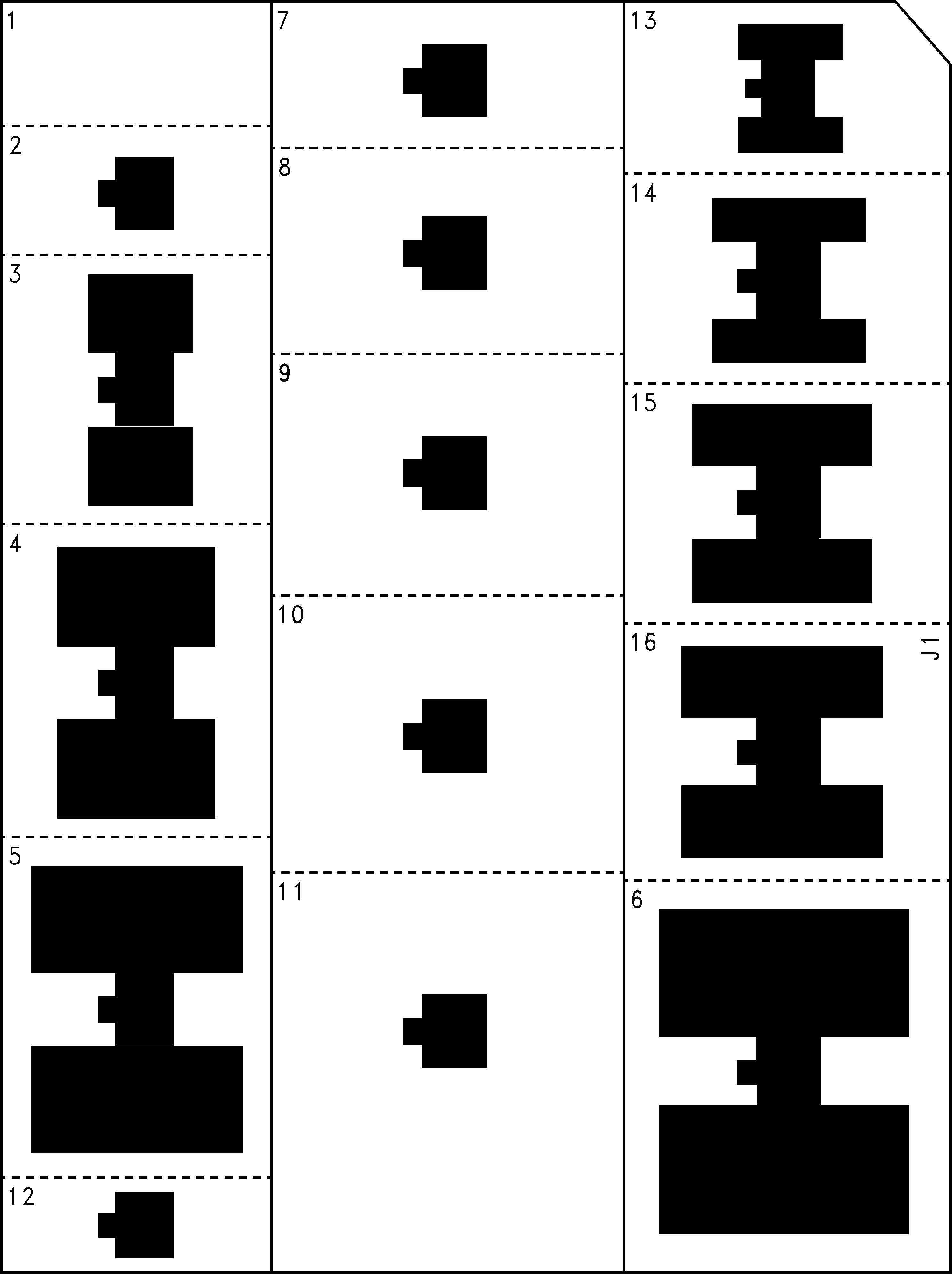 Figure 9-18 Bottom View of the Thermal Test Pattern in Actual Scale