SNOS412Q February 2000 – January 2023 LM1117
PRODUCTION DATA
- 1 Features
- 2 Applications
- 3 Description
- 4 Revision History
- 5 Device Comparison Table
- 6 Pin Configuration and Functions
- 7 Specifications
- 8 Detailed Description
- 9 Application and Implementation
- 10Device and Documentation Support
- 11Mechanical, Packaging, and Orderable Information
Package Options
Mechanical Data (Package|Pins)
Thermal pad, mechanical data (Package|Pins)
Orderable Information
6 Pin Configuration and Functions
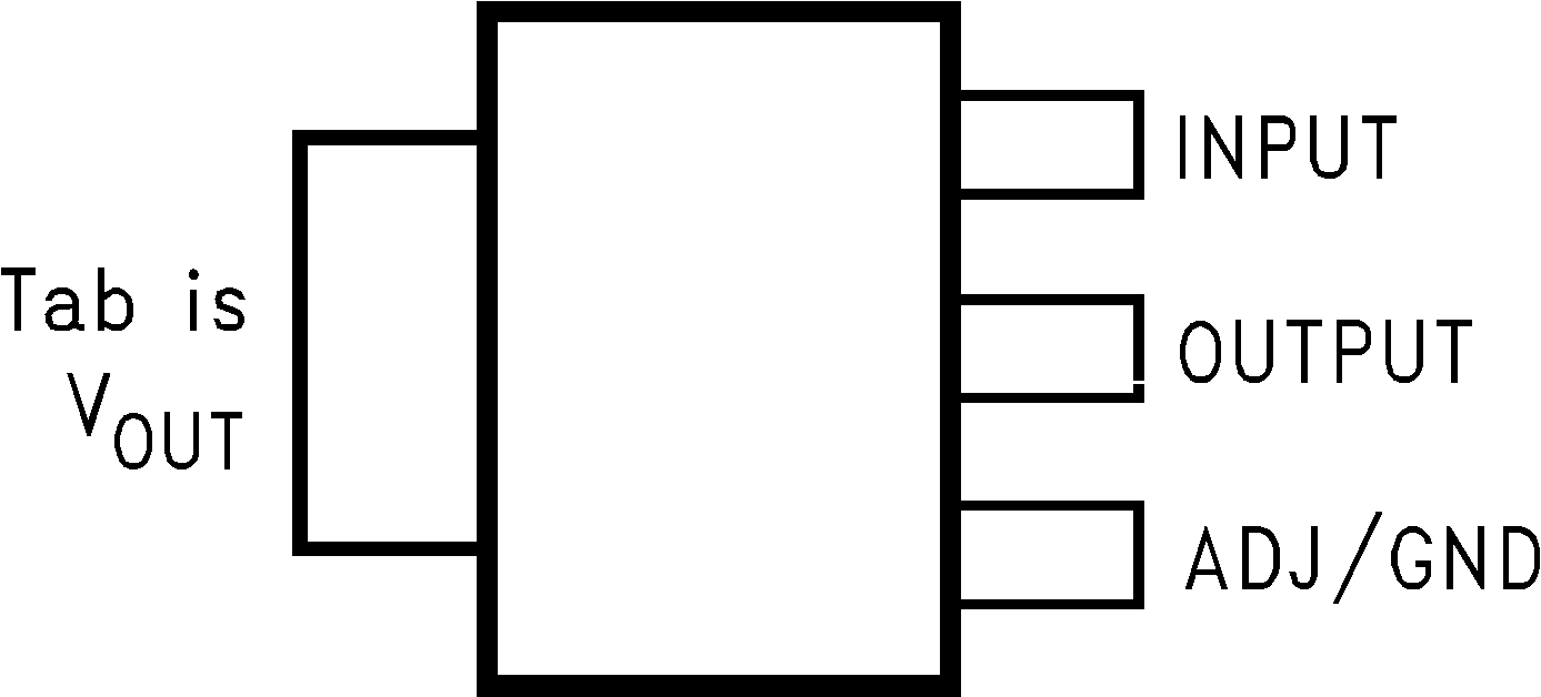
 Figure 6-1 DCY Package,4-Pin SOT(Top View)
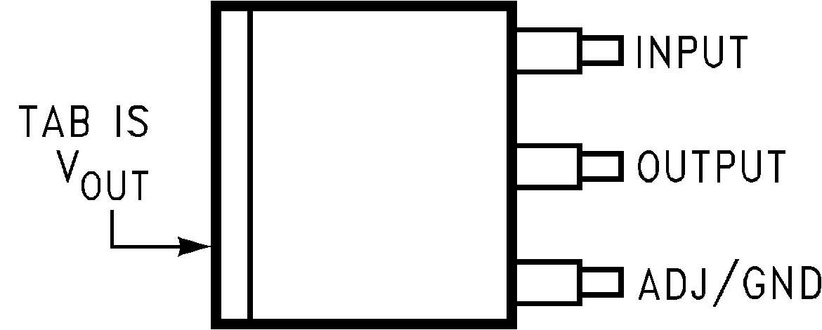
 Figure 6-3 KTT Package,3-Pin TO-263(Top View)
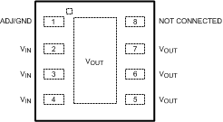
When using
the WSON package pins 2, 3, and 4 must be connected together and pins 5, 6,
and 7 must be connected together.
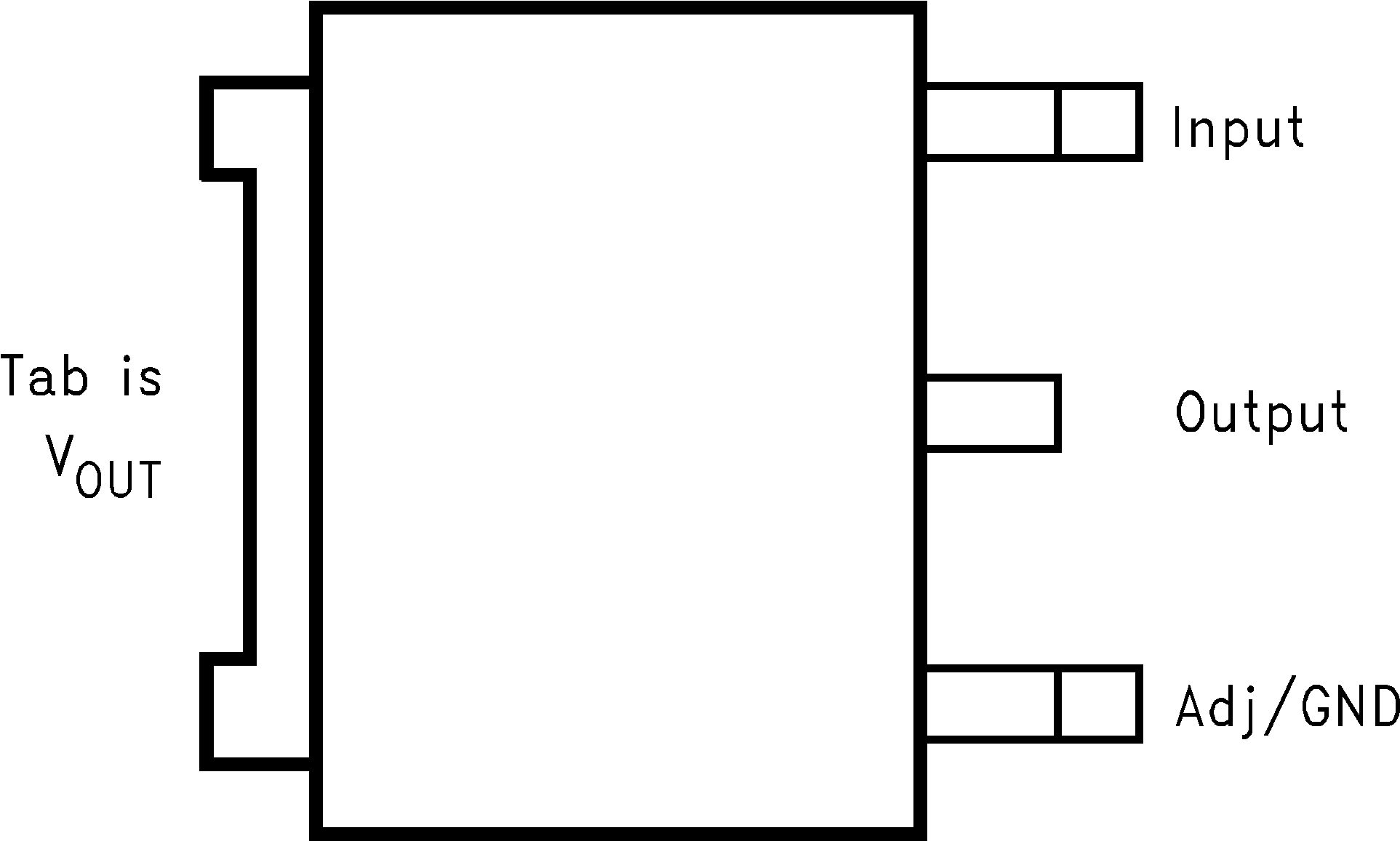
Figure 6-5 NGN Package,8-Pin WSON(Top View) Figure 6-2 NDE Package,3-Pin TO-220(Top View)
 Figure 6-4 NDP Package,3-Pin TO-252(Top View)
Table 6-1 Pin Functions
| PIN | I/O | DESCRIPTION | |||||
|---|---|---|---|---|---|---|---|
| NAME | TO-252 | WSON | SOT-223 | TO-263 | TO-220 | ||
| ADJ/GND | 1 | 1 | 1 | 1 | 1 | — | Adjust pin for adjustable output option. Ground pin for fixed output option. |
| VIN | 3 | 2, 3, 4 | 3 | 3 | 3 | I | Input voltage pin for the regulator |
| VOUT | 2 , TAB | 5, 6, 7, TAB | 2, 4 | 2, TAB | 2, TAB | O | Output voltage pin for the regulator |