SNOS412Q February 2000 – January 2023 LM1117
PRODUCTION DATA
- 1 Features
- 2 Applications
- 3 Description
- 4 Revision History
- 5 Device Comparison Table
- 6 Pin Configuration and Functions
- 7 Specifications
- 8 Detailed Description
- 9 Application and Implementation
- 10Device and Documentation Support
- 11Mechanical, Packaging, and Orderable Information
Package Options
Mechanical Data (Package|Pins)
Thermal pad, mechanical data (Package|Pins)
- KTT|3
Orderable Information
8.4.1 Protection Diodes
Under normal operation, the LM1117 regulators do not need any protection diode. With the adjustable device, the internal resistance between the adjust and output terminals limits the current. No diode is needed to divert the current around the regulator even with capacitor on the adjust terminal. The adjust pin can take a transient signal of ±25V with respect to the output voltage without damaging the device.
When a output capacitor is connected to a regulator and the input is shorted to ground, the output capacitor will discharge into the output of the regulator. The discharge current depends on the value of the capacitor, the output voltage of the regulator, and rate of decrease of VIN. In the LM1117 regulators, the internal diode between the output and input pins can withstand microsecond surge currents of 10A to 20A. With an extremely large output capacitor (≥1000 µF), and with input instantaneously shorted to ground, the regulator could be damaged.
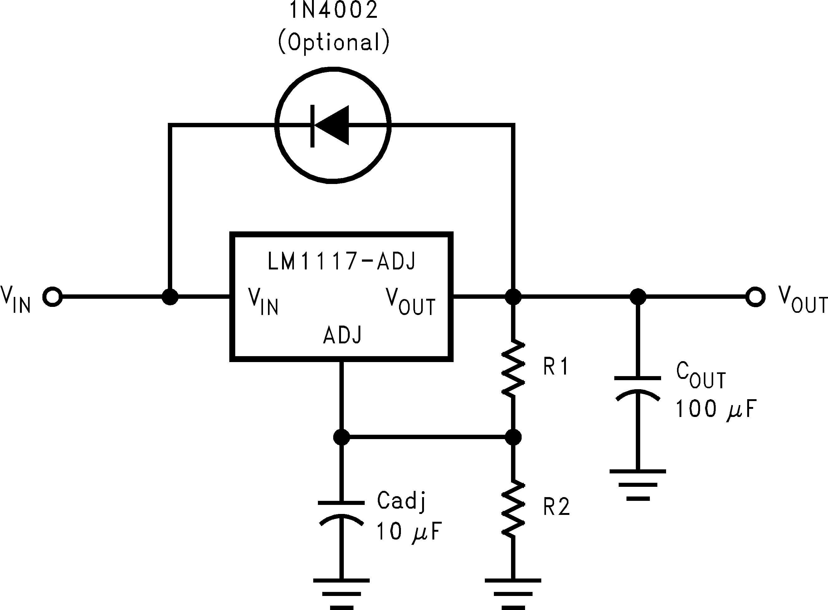
In this case, an external diode is recommended between the output and input pins to protect the regulator, as shown in Figure 8-4.
 Figure 8-4 Regulator With Protection Diode