SNVS625G February 2011 – March 2022 LM21215
PRODUCTION DATA
- 1 Features
- 2 Applications
- 3 Description
- 4 Revision History
- 5 Pin Configuration and Functions
- 6 Specifications
- 7 Detailed Description
- 8 Application and Implementation
- 9 Layout
- 10Device and Documentation Support
- 11Mechanical, Packaging, and Orderable Information
Package Options
Mechanical Data (Package|Pins)
- PWP|20
Thermal pad, mechanical data (Package|Pins)
- PWP|20
Orderable Information
8.2.1.2.6 Output Capacitor Selection
The output capacitor, COUT, filters the inductor ripple current and provides a source of charge for transient load conditions. A wide range of output capacitors can be used with the LM21215 that provide various advantages. The best performance is typically obtained using ceramic, SP, or OSCON type chemistries. Typical trade-offs are that the ceramic capacitor provides extremely low ESR to reduce the output ripple voltage and noise spikes, while the SP and OSCON capacitors provide a large bulk capacitance in a small volume for transient loading conditions.
When selecting the value for the output capacitor, the two performance characteristics to consider are the output voltage ripple and transient response. The output voltage ripple can be approximated by using Equation 6:

where
- ΔVOUT (V) is the amount of peak-to-peak voltage ripple at the power supply output.
- RESR (Ω) is the series resistance of the output capacitor.
- fSW (Hz) is the switching frequency.
- COUT (F) is the output capacitance used in the design.
The amount of output ripple that can be tolerated is application specific, however, a general recommendation is to keep the output ripple less than 1% of the rated output voltage. Keep in mind ceramic capacitors are sometimes preferred because they have very low ESR, however, depending on package and voltage rating of the capacitor, the value of the capacitance can drop significantly with applied voltage. The output capacitor selection will also affect the output voltage droop during a load transient. The peak droop on the output voltage during a load transient is dependent on many factors, however, an approximation of the transient droop ignoring loop bandwidth can be obtained using Equation 7:
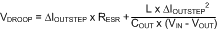
where
- COUT (F) is the minimum required output capacitance.
- L (H) is the value of the inductor.
- VDROOP (V) is the output voltage drop ignoring loop bandwidth considerations.
- ΔIOUTSTEP (A) is the load step change.
- RESR (Ω) is the output capacitor ESR.
- VIN (V) is the input voltage.
- VOUT (V) is the set regulator output voltage.
Examine both the tolerance and voltage coefficient of the capacitor when designing for a specific output ripple or transient droop target.