SNVS625G February   2011  – March 2022 LM21215

PRODUCTION DATA  

  1. Features
  2. Applications
  3. Description
  4. Revision History
  5. Pin Configuration and Functions
  6. Specifications
    1. 6.1 Absolute Maximum Ratings
    2. 6.2 ESD Ratings
    3. 6.3 Recommended Operating Ratings
    4. 6.4 Electrical Characteristics
    5. 6.5 Typical Characteristics
  7. Detailed Description
    1. 7.1 Overview
    2. 7.2 Functional Block Diagram
    3. 7.3 Feature Description
      1. 7.3.1 Precision Enable
      2. 7.3.2 UVLO
      3. 7.3.3 Current Limit
      4. 7.3.4 Short-Circuit Protection
      5. 7.3.5 Thermal Protection
      6. 7.3.6 Light Load Operation
      7. 7.3.7 Power Good Flag
    4. 7.4 Device Functional Modes
  8. Application and Implementation
    1. 8.1 Application Information
    2. 8.2 Typical Application
      1. 8.2.1 Typical Application 1
        1. 8.2.1.1 Design Requirements
        2. 8.2.1.2 Detailed Design Procedure
          1. 8.2.1.2.1 Custom Design With WEBENCH® Tools
          2. 8.2.1.2.2 Output Voltage
          3. 8.2.1.2.3 Precision Enable
          4. 8.2.1.2.4 Soft Start
          5. 8.2.1.2.5 Inductor Selection
          6. 8.2.1.2.6 Output Capacitor Selection
          7. 8.2.1.2.7 Input Capacitor Selection
          8. 8.2.1.2.8 Programmable Current Limit
          9. 8.2.1.2.9 Control Loop Compensation
        3. 8.2.1.3 Application Curves
      2. 8.2.2 Typical Application Schematic 2
        1. 8.2.2.1 Design Requirements
        2. 8.2.2.2 Detailed Design Procedure
  9. Layout
    1. 9.1 Layout Considerations
    2. 9.2 Layout Example
      1. 9.2.1 Thermal Considerations
  10. 10Device and Documentation Support
    1. 10.1 Device Support
      1. 10.1.1 Third-Party Products Disclaimer
      2. 10.1.2 Development Support
        1. 10.1.2.1 Custom Design With WEBENCH® Tools
    2. 10.2 Receiving Notification of Documentation Updates
    3. 10.3 Support Resources
    4. 10.4 Trademarks
    5. 10.5 Electrostatic Discharge Caution
    6. 10.6 Glossary
  11. 11Mechanical, Packaging, and Orderable Information

Package Options

Mechanical Data (Package|Pins)
Thermal pad, mechanical data (Package|Pins)
Orderable Information
Programmable Current Limit

A resistor from the ILIM pin to GND sets the internal current limit on the LM21215. Program the current limit so that the peak inductor current (IL) does not trigger the current limit in normal operation. This requires setting the resistor from the ILIM pin to GND (RILIM) to the appropriate value to allow the maximum ripple current, ΔILMAX plus the DC output current through the high-side FET during normal operation. The maximum ripple current can be described as:
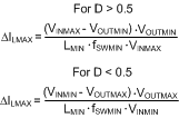
Equation 9. GUID-46AE8B67-3B44-47D3-BB3E-B6E00AE3210C-low.gif

where

  • VINMAX, VINMIN, VOUTMAX, VOUTMIN, LMIN, and FSWMIN are the respective maximum and minimum conditions of the system as defined by the component tolerance and device variation.

From this, the maximum allowable current through the high-side FET (IHSMAX) of device can be described as:

Equation 10. GUID-D7A93CD7-4576-47A6-B667-08D3C1CDAF14-low.gif

where

  • IOUTMAX is the maximum defined DC output current, up to 15 A.

Once the IHSMAX value has been determined, a nominal value of the RILIM resistor can be calculated as follows:
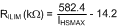
Equation 11. GUID-7BBD42A6-B16D-409F-BC68-8C405E63291B-low.gif

where

  • RILIM value is the nominal resistance necessary for the given IHSMAX value.

A conservative design should also take into account the device variation over VIN and temperature, as seen in the Electrical Characteristics for the ICLR parameter and the typical performance characteristics. These variations can cause the IHSMAX value to increase, depending on the range of the input voltage and junction temperature.