SNVS625G February   2011  – March 2022 LM21215

PRODUCTION DATA  

  1. Features
  2. Applications
  3. Description
  4. Revision History
  5. Pin Configuration and Functions
  6. Specifications
    1. 6.1 Absolute Maximum Ratings
    2. 6.2 ESD Ratings
    3. 6.3 Recommended Operating Ratings
    4. 6.4 Electrical Characteristics
    5. 6.5 Typical Characteristics
  7. Detailed Description
    1. 7.1 Overview
    2. 7.2 Functional Block Diagram
    3. 7.3 Feature Description
      1. 7.3.1 Precision Enable
      2. 7.3.2 UVLO
      3. 7.3.3 Current Limit
      4. 7.3.4 Short-Circuit Protection
      5. 7.3.5 Thermal Protection
      6. 7.3.6 Light Load Operation
      7. 7.3.7 Power Good Flag
    4. 7.4 Device Functional Modes
  8. Application and Implementation
    1. 8.1 Application Information
    2. 8.2 Typical Application
      1. 8.2.1 Typical Application 1
        1. 8.2.1.1 Design Requirements
        2. 8.2.1.2 Detailed Design Procedure
          1. 8.2.1.2.1 Custom Design With WEBENCH® Tools
          2. 8.2.1.2.2 Output Voltage
          3. 8.2.1.2.3 Precision Enable
          4. 8.2.1.2.4 Soft Start
          5. 8.2.1.2.5 Inductor Selection
          6. 8.2.1.2.6 Output Capacitor Selection
          7. 8.2.1.2.7 Input Capacitor Selection
          8. 8.2.1.2.8 Programmable Current Limit
          9. 8.2.1.2.9 Control Loop Compensation
        3. 8.2.1.3 Application Curves
      2. 8.2.2 Typical Application Schematic 2
        1. 8.2.2.1 Design Requirements
        2. 8.2.2.2 Detailed Design Procedure
  9. Layout
    1. 9.1 Layout Considerations
    2. 9.2 Layout Example
      1. 9.2.1 Thermal Considerations
  10. 10Device and Documentation Support
    1. 10.1 Device Support
      1. 10.1.1 Third-Party Products Disclaimer
      2. 10.1.2 Development Support
        1. 10.1.2.1 Custom Design With WEBENCH® Tools
    2. 10.2 Receiving Notification of Documentation Updates
    3. 10.3 Support Resources
    4. 10.4 Trademarks
    5. 10.5 Electrostatic Discharge Caution
    6. 10.6 Glossary
  11. 11Mechanical, Packaging, and Orderable Information

Package Options

Mechanical Data (Package|Pins)
Thermal pad, mechanical data (Package|Pins)
Orderable Information

Typical Characteristics

Unless otherwise specified: VIN = 5 V, VOUT = 1.2 V, L= 0.56 µH (1.8-mΩ RDCR), CSS = 33 nF, TA = 25°C for efficiency curves, loop gain plots and waveforms, and TJ = 25°C for all others.
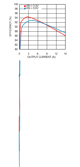
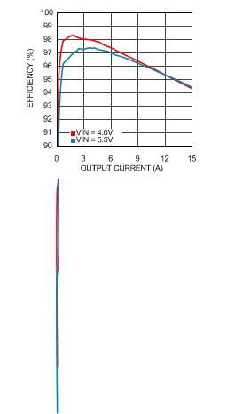
GUID-17081102-A169-4878-852D-D2807DECADBD-low.gifFigure 6-1 Efficiency
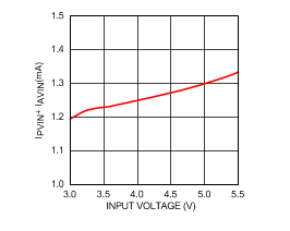
GUID-26B6129A-AD7F-475F-A334-6D0D445A21BA-low.gifFigure 6-3 Non-Switching IQTOTAL vs VIN
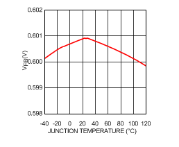
GUID-953FCA4C-E793-4D3F-94C6-817405B4951F-low.gifFigure 6-5 VFB vs Temperature
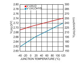
GUID-33DAFC67-284E-4F7A-9828-4BA931E63336-low.gifFigure 6-7 UVLO Threshold and Hysteresis vs Temperature
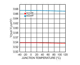
GUID-72C4942A-FD9B-4299-87D9-D46C74A9173E-low.gifFigure 6-9 OVP/UVP Threshold vs Temperature
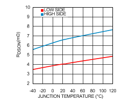
GUID-3B005BF6-AD1C-41EC-80A9-FC9941D2B6C9-low.gifFigure 6-11 FET Resistance vs Temperature
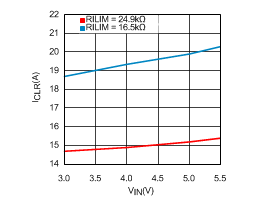
GUID-92D56344-C7FE-4D78-B69D-2598C7DE0643-low.gifFigure 6-13 Peak Current Limit (ICLR) vs VIN
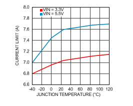
GUID-CF4DE3B4-F404-4331-9467-08B4C124E171-low.gif
RILIM = 61.9 KΩ
Figure 6-15 Peak Current Limit (ICLR) vs Temperature
GUID-BBFF4D59-5902-49DC-8358-72A76CAD936B-low.gif
200 µs/DIV
                                            200 µs/DIV
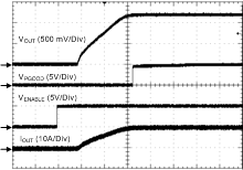
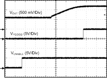
Figure 6-17 Start-up With SS/TRK Open Circuit
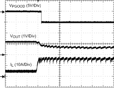
GUID-6DC46A1D-ECDC-41F6-93D2-859640C11D63-low.gif
100 µs/DIVRILIM = 20 KΩ
Figure 6-19 Output Overcurrent Condition
GUID-E13023DA-5805-43D6-BCF6-14B1C7F9AAB5-low.gif
VOUT = 3.3 VInductor P/N SER2010-02MLD
Figure 6-2 Efficiency
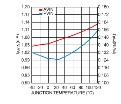
GUID-F28F73A0-8E9D-4F75-AD42-A821812891F3-low.gifFigure 6-4 Non-Switching IAVIN and IPVIN vs Temperature
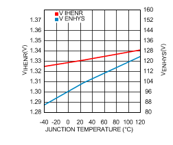
GUID-B7E6576E-BA9F-43DA-A826-7819BCA71A1D-low.gifFigure 6-6 Enable Threshold and Hysteresis vs Temperature
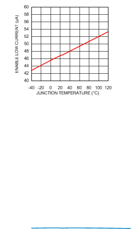
GUID-4C6D96BA-8D7D-46B8-947D-0B4490E00EC8-low.gifFigure 6-8 Enable Low Current vs Temperature
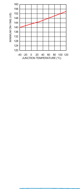
GUID-60653A88-E62C-4105-A529-0F9D4ADF2D40-low.gifFigure 6-10 Minimum On-Time vs Temperature
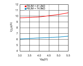
GUID-A1BCB9F5-B486-4D95-AFD5-CCE7E78D6B74-low.gifFigure 6-12 Peak Current Limit (ICLR) vs VIN
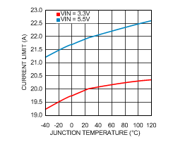
GUID-F66A9B5B-A76A-4DCF-B687-8A88301CD874-low.gif
RILIM = 10 KΩ
Figure 6-14 Peak Current Limit (ICLR) vs Temperature
GUID-97892607-FC27-48EA-B1E6-62DA90E67DC1-low.gif
  2 ms/DIV
Figure 6-16 Start-up With Prebiased Output
GUID-2DA8FF3B-4101-4087-AA1C-0C4C8A6CCF1D-low.gif
100 µs/DIV
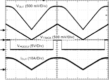
Figure 6-18 Start-up With Applied Track Signal