SNVS625G February 2011 – March 2022 LM21215
PRODUCTION DATA
- 1 Features
- 2 Applications
- 3 Description
- 4 Revision History
- 5 Pin Configuration and Functions
- 6 Specifications
- 7 Detailed Description
- 8 Application and Implementation
- 9 Layout
- 10Device and Documentation Support
- 11Mechanical, Packaging, and Orderable Information
Package Options
Mechanical Data (Package|Pins)
- PWP|20
Thermal pad, mechanical data (Package|Pins)
- PWP|20
Orderable Information
8.2.1.2.7 Input Capacitor Selection
Quality input capacitors are necessary to limit the ripple voltage at the VIN pin while supplying most of the switch current during the on time. Additionally, they help minimize input voltage droop in an output current transient condition. In general, it is recommended to use a ceramic capacitor for the input as it provides both a low impedance and small footprint. Use of a high grade dielectric for the ceramic capacitor, such as X5R or X7R, will provide improved overtemperature performance and also minimize the DC voltage derating that occurs with Y5V capacitors. The input capacitors CIN1 and CIN2 must be placed as close as possible to the PVIN and PGND pins.
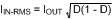
Select non-ceramic input capacitors for RMS current rating and minimum ripple voltage. A good approximation for the required ripple current rating is given by the relationship:
As indicated by the RMS ripple current equation, the highest requirement for RMS current rating occurs at 50% duty cycle. For this case, the RMS ripple current rating of the input capacitor should be greater than half the output current. For best performance, low-ESR ceramic capacitors should be placed in parallel with higher capacitance capacitors to provide the best input filtering for the device.
When operating at low input voltages (3.3 V or lower), additional capacitance can be necessary to protect from triggering an undervoltage condition on an output current transient. This will depend on the impedance between the input voltage supply and the LM21215, as well as the magnitude and slew rate of the output transient.
The AVIN pin requires a 1-µF ceramic capacitor to AGND and a 1-Ω resistor to PVIN. This RC network filters inherent noise on PVIN from the sensitive analog circuitry connected to AVIN.