SNVS625G February 2011 – March 2022 LM21215
PRODUCTION DATA
- 1 Features
- 2 Applications
- 3 Description
- 4 Revision History
- 5 Pin Configuration and Functions
- 6 Specifications
- 7 Detailed Description
- 8 Application and Implementation
- 9 Layout
- 10Device and Documentation Support
- 11Mechanical, Packaging, and Orderable Information
Package Options
Mechanical Data (Package|Pins)
- PWP|20
Thermal pad, mechanical data (Package|Pins)
- PWP|20
Orderable Information
3 Description
The LM21215 is a monolithic synchronous point-of-load buck regulator that is capable of delivering up to 15 A of continuous output current while producing an output voltage down to 0.6 V with outstanding efficiency. The device is optimized to work over an input voltage range of 2.95 V to 5.5 V, making it suitable for a wide variety of low voltage systems. The voltage mode control loop provides high noise immunity, narrow duty cycle capability and can be compensated to be stable with any type of output capacitance, providing maximum flexibility and ease of use.
The LM21215 features internal overvoltage protection (OVP) and resistor-programmable overcurrent protection (OCP) for increased system reliability. A precision enable pin and integrated UVLO allow turn-on of the device to be tightly controlled and sequenced. Start-up inrush currents are limited by both an internally fixed and externally adjustable soft-start circuit. Fault detection and supply sequencing are possible with the integrated power good circuit.
The LM21215 is designed to work well in multi-rail power supply architectures. The output voltage of the device can be configured to track an external voltage rail using the SS/TRK pin. If the output is prebiased at start-up, it will not sink current, allowing the output to smoothly rise past the prebiased voltage. The regulator is offered in a 20-pin HTSSOP package with an exposed pad that can be soldered to the PCB, eliminating the need for bulky heat sinks.
| PART NUMBER | PACKAGE(1) | BODY SIZE (NOM) |
|---|---|---|
| LM21215 | HTSSOP (20) | 6.50 mm × 4.40 mm |
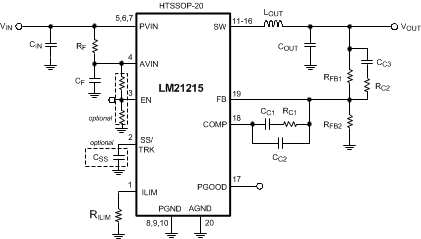
 Simplified Application
Circuit