SNVS625G February 2011 – March 2022 LM21215
PRODUCTION DATA
- 1 Features
- 2 Applications
- 3 Description
- 4 Revision History
- 5 Pin Configuration and Functions
- 6 Specifications
- 7 Detailed Description
- 8 Application and Implementation
- 9 Layout
- 10Device and Documentation Support
- 11Mechanical, Packaging, and Orderable Information
Package Options
Mechanical Data (Package|Pins)
- PWP|20
Thermal pad, mechanical data (Package|Pins)
- PWP|20
Orderable Information
8.2.1.2.4 Soft Start
When EN has exceeded 1.35 V, and both PVIN and AVIN have exceeded the UVLO threshold, the LM21215 begins charging the output linearly to the voltage level dictated by the feedback resistor network. The LM21215 employs a user-adjustable soft-start circuit to lengthen the charging time of the output set by a capacitor from the soft-start pin to ground. After enable exceeds 1.35 V, an internal 2-µA current source begins to charge the soft-start capacitor. This allows the user to limit inrush currents due to a high output capacitance and not cause an overcurrent condition. Adding a soft-start capacitor can also reduce the stress on the input rail. Larger capacitor values will result in longer start-up times. Use Equation 4 to approximate the size of the soft-start capacitor:

where
- ISS is nominally 2 µA.
- tSS is the desired start-up time.
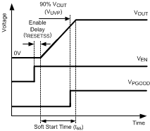
If VIN is higher than the UVLO level and enable is toggled high the soft start sequence begins. There is a small delay between enable transitioning high and the beginning of the soft start sequence. This delay allows the LM21215 to initialize its internal circuitry. Once the output has charged to 90% of the nominal output voltage the power-good flag transitions high. This behavior is illustrated in Figure 8-4.
 Figure 8-4 Soft-Start Timing
As shown above, the size of the capacitor is influenced by the nominal feedback voltage level 0.6 V, the soft-start charging current, ISS (2 µA), and the desired soft-start time. If no soft-start capacitor is used, then the LM21215 defaults to a minimum start-up time of 500 µs. The LM21215 does not start up faster than 500 µs. When enable is cycled or the device enters UVLO, the charge developed on the soft-start capacitor is discharged to reset the start-up process. This also happens when the device enters short circuit mode from an overcurrent event.