SNVS032E February 2000 – January 2016 LM2651
PRODUCTION DATA.
- 1 Features
- 2 Applications
- 3 Description
- 4 Revision History
- 5 Pin Configuration and Functions
- 6 Specifications
- 7 Detailed Description
- 8 Application and Implementation
- 9 Power Supply Recommendations
- 10Layout
- 11Device and Documentation Support
- 12Mechanical, Packaging, and Orderable Information
Package Options
Mechanical Data (Package|Pins)
- PW|16
Thermal pad, mechanical data (Package|Pins)
Orderable Information
8 Application and Implementation
NOTE
Information in the following applications sections is not part of the TI component specification, and TI does not warrant its accuracy or completeness. TI’s customers are responsible for determining suitability of components for their purposes. Customers should validate and test their design implementation to confirm system functionality.
8.1 Application Information
LM2651 operates in a constant frequency (300 kHz), current-mode PWM for moderate to heavy loads; and it automatically switches to hysteretic mode for light loads. The current of the top switch is sensed by a patented internal circuitry. This unique technique gets rid of the external sense resistor, saves cost and size, and improves noise immunity of the sensed current. A feed forward from the input voltage is added to reduce the variation of the current limit over the input voltage range.
8.2 Typical Application
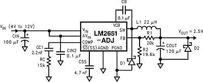
 Figure 11. Schematic for the Typical Board Layout
8.2.1 Design Requirements
To properly size the components for the application, the designer needs the following parameters: input voltage range, output voltage, output current range, and the switching frequency. These four main parameters affect the choices of component available to achieve a proper system behavior. TI recommends a Schottky diode to prevent the intrinsic body diode of the low-side MOSFET from conducting during deadtime. See Detailed Design Procedure for more information.
8.2.2 Detailed Design Procedure
This section presents guidelines for selecting external components.
8.2.2.1 Input Capacitor
A low ESR aluminum, tantalum, or ceramic capacitor is needed between the input pin and power ground. This capacitor prevents large voltage transients from appearing at the input. The capacitor is selected based on the RMS current and voltage requirements. The RMS current is given by Equation 1.

The RMS current reaches its maximum (IOUT/2) when VIN equals 2 VOUT. For an aluminum or ceramic capacitor, the voltage rating should be at least 25% higher than the maximum input voltage. If a tantalum capacitor is used, the voltage rating required is about twice the maximum input voltage. The tantalum capacitor should be surge-current tested by the manufacturer to prevent being shorted by the inrush current. TI also recommends putting a small ceramic capacitor (0.1 μF) between the input pin and ground pin to reduce high-frequency spikes.
8.2.2.2 Inductor
The most critical parameters for the inductor are the inductance, peak current, and the DC resistance. The inductance is related to the peak-to-peak inductor ripple current, the input and the output voltages, as given by Equation 2.

A higher value of ripple current reduces inductance, but increases the conductance loss, core loss, current stress for the inductor and switch devices. It also requires a bigger output capacitor for the same output voltage ripple requirement. A reasonable value is setting the ripple current to be 30% of the DC output current. Since the ripple current increases with the input voltage, the maximum input voltage is always used to determine the inductance. The DC resistance of the inductor is a key parameter for the efficiency. Lower DC resistance is available with a bigger winding area. A good tradeoff between the efficiency and the core size is letting the inductor copper loss equal 2% of the output power.
8.2.2.3 Output Capacitor
The selection of COUT is driven by the maximum allowable output voltage ripple. The output ripple in the constant frequency, PWM mode is approximated by using Equation 3.

The ESR term usually plays the dominant role in determining the voltage ripple. A low ESR aluminum electrolytic or tantalum capacitor (such as Nichicon PL series, Sanyo OS-CON, Sprague 593D, 594D, AVX TPS, and CDE polymer aluminum) is recommended. An electrolytic capacitor is not recommended for temperatures below −25°C since its ESR rises dramatically at cold temperature. A tantalum capacitor has a much better ESR specification at cold temperature and is preferred for low temperature applications.
The output voltage ripple in constant frequency mode has to be less than the sleep mode voltage hysteresis to avoid entering the sleep mode at full load as given by Equation 4.
8.2.2.4 Boost Capacitor
TI recommends a 0.1-μF ceramic capacitor for the boost capacitor. The typical voltage across the boost capacitor is 6.7 V.
8.2.2.5 Soft-Start Capacitor
A soft-start capacitor is used to provide the soft-start feature. When the input voltage is first applied, or when the SD(SS) pin is allowed to go high, the soft-start capacitor is charged by a current source (approximately 2 μA). When the SD(SS) pin voltage reaches 0.6 V (shutdown threshold), the internal regulator circuitry starts to operate. The current charging the soft-start capacitor increases from 2 μA to approximately 10 μA. With the SD(SS) pin voltage between 0.6 V and 1.3 V, the level of the current limit is zero, which means the output voltage is still zero. When the SD(SS) pin voltage increases beyond 1.3 V, the current limit starts to increase. The switch duty cycle, which is controlled by the level of the current limit, starts with narrow pulses and gradually gets wider. At the same time, the output voltage of the converter increases towards the nominal value, which brings down the output voltage of the error amplifier. When the output of the error amplifier is less than the current limit voltage, it takes over the control of the duty cycle. The converter enters the normal current-mode PWM operation. The SD(SS) pin voltage is eventually charged up to about 2 V.
The soft-start time can be estimated using Equation 5.
8.2.2.6 R1 and R2 (Programming Output Voltage)
Use Equation 6 to select the appropriate resistor values.
where
- VREF = 1.238 V
Select resistors between 10 kΩ and 100 kΩ. (1% or higher accuracy metal film resistors for R1 and R2.)
8.2.2.7 Compensation Components
In the control to output transfer function, the first pole Fp1 can be estimated as 1/(2πROUTCOUT); The ESR zero Fz1 of the output capacitor is 1/(2πESRCOUT); Also, there is a high-frequency pole Fp2 in the range of 45 kHz to 150 kHz as given by Equation 7.
where
- D = VOUT/VIN
- n = 1+0.348L/(VIN−VOUT) (L is in µHs and VIN and VOUT in volts).
The total loop gain G is approximately 500/IOUT where IOUT is in amperes.
A Gm amplifier is used inside the LM2651. The output resistor Ro of the Gm amplifier is about 80 kΩ. Cc1 and RC together with Ro give a lag compensation to roll off the gain as given by Equation 8.
In some applications, the ESR zero Fz1 cannot be cancelled by Fp2. Then, Cc2 is needed to introduce Fpc2 to cancel the ESR zero, Fp2 = 1/(2πCc2Ro‖Rc).
The rule of thumb is to have more than 45° phase margin at the crossover frequency (G = 1).
If COUT is higher than 68 µF, Cc1 = 2.2 nF, and Rc = 15 kΩ are good choices for most applications. If the ESR zero is too low to be cancelled by Fp2, add Cc2.
If the transient response to a step load is important, choose RC to be higher than 10 kΩ.
8.2.2.8 External Schottky Diode
TI recommends a Schottky diode D1 to prevent the intrinsic body diode of the low-side MOSFET from conducting during the deadtime in PWM operation and hysteretic mode when both MOSFETs are off. If the body diode turns on, there is extra power dissipation in the body diode because of the reverse-recovery current and higher forward voltage; the high-side MOSFET also has more switching loss since the negative diode reverse-recovery current appears as the high-side MOSFET turnon current in addition to the load current. These losses degrade the efficiency by 1–2%. The improved efficiency and noise immunity with the Schottky diode become more obvious with increasing input voltage and load current.
The breakdown voltage rating of D1 is preferred to be 25% higher than the maximum input voltage. Since D1 is only on for a short period of time, the average current rating for D1 only requires being higher than 30% of the maximum output current. It is important to place D1 very close to the drain and source of the low-side MOSFET, extra parasitic inductance in the parallel loop slows the turnon of D1 and direct the current through the body diode of the low-side MOSFET.
When an undervoltage situation occurs, the output voltage can be pulled below ground as the inductor current is reversed through the synchronous FET. For applications that require protection from a negative voltage, TI recommends a clamping diode D2. When used, D2 should be connected cathode to VOUT and anode to ground. TI recommends a diode rated for a minimum of 2 A.
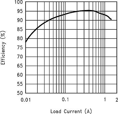
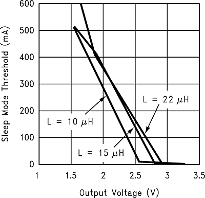
8.2.3 Application Curves

| (VIN = 5 V, VOUT = 3.3 V) | ||

For ADJ Version (VIN = 5 V)