SNVS032E February 2000 – January 2016 LM2651
PRODUCTION DATA.
- 1 Features
- 2 Applications
- 3 Description
- 4 Revision History
- 5 Pin Configuration and Functions
- 6 Specifications
- 7 Detailed Description
- 8 Application and Implementation
- 9 Power Supply Recommendations
- 10Layout
- 11Device and Documentation Support
- 12Mechanical, Packaging, and Orderable Information
Package Options
Mechanical Data (Package|Pins)
- PW|16
Thermal pad, mechanical data (Package|Pins)
Orderable Information
10 Layout
10.1 Layout Guidelines
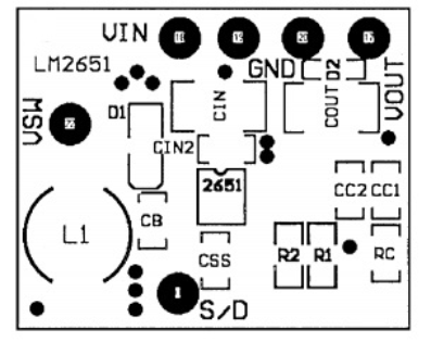
Layout is critical to reduce noises and ensure specified performance. The important guidelines are listed as follows:
- Minimize the parasitic inductance in the loop of input capacitors and the internal MOSFETs by connecting the input capacitors to VIN and PGND pins with short and wide traces. This is important because the rapidly switching current, together with wiring inductance can generate large voltage spikes that may result in noise problems.
- Minimize the trace from the center of the output resistor divider to the FB pin and keep it away from noise sources to avoid noise pickup. For applications requiring tight regulation at the output, TI recommends a dedicated sense trace (separated from the power trace) to connect the top of the resistor divider to the output.
- If the Schottky diode D1 is used, minimize the traces connecting D1 to SW and PGND pins.
10.2 Layout Example
 Figure 14. LM2651 Layout Recommendation