SNVS032E February 2000 – January 2016 LM2651
PRODUCTION DATA.
- 1 Features
- 2 Applications
- 3 Description
- 4 Revision History
- 5 Pin Configuration and Functions
- 6 Specifications
- 7 Detailed Description
- 8 Application and Implementation
- 9 Power Supply Recommendations
- 10Layout
- 11Device and Documentation Support
- 12Mechanical, Packaging, and Orderable Information
Package Options
Mechanical Data (Package|Pins)
- PW|16
Thermal pad, mechanical data (Package|Pins)
Orderable Information
7 Detailed Description
7.1 Overview
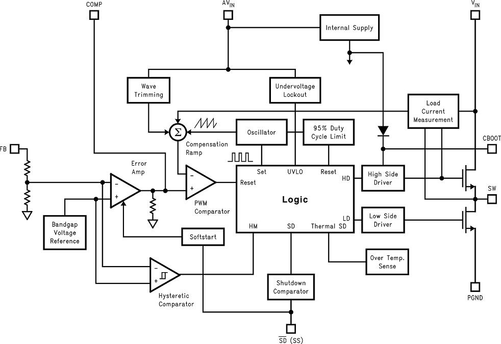
The LM2651 operates in a constant frequency (300 kHz), current-mode PWM for moderate to heavy loads, and automatically switches to hysteretic mode for light loads. In hysteretic mode, the switching frequency is reduced to maintain high efficiency.
7.2 Functional Block Diagram

7.3 Feature Description
When the load current is higher than the sleep mode threshold, the part is always operating in PWM mode. At the beginning of each switching cycle, the high-side switch is turned on, the current from the high-side switch is sensed and compared with the output of the error amplifier (COMP pin). When the sensed current reaches the COMP pin voltage level, the high-side switch is turned off; after 40 ns (deadtime), the low-side switch is turned on. At the end of the switching cycle, the low-side switch is turned off; and the same cycle repeats.
When the load current decreases below the sleep mode threshold, the output voltage rises slightly, this rise is sensed by the hysteretic mode comparator which makes the part go into the hysteretic mode with both the high and low side switches off. The output voltage starts to drop until it hits the low threshold of the hysteretic comparator, and the part immediately goes back to the PWM operation. The output voltage keeps increasing until it reaches the top hysteretic threshold, then both the high- and low-side switches turn off again, and the cycle repeats.
7.4 Device Functional Modes
The cycle-by-cycle current limit circuitry turns off the high-side MOSFET whenever the current in MOSFET reaches 2 A. A shutdown pin is available to disable the LM2651 and reduce the supply current to 7 µA.