SNVS032E February 2000 – January 2016 LM2651
PRODUCTION DATA.
- 1 Features
- 2 Applications
- 3 Description
- 4 Revision History
- 5 Pin Configuration and Functions
- 6 Specifications
- 7 Detailed Description
- 8 Application and Implementation
- 9 Power Supply Recommendations
- 10Layout
- 11Device and Documentation Support
- 12Mechanical, Packaging, and Orderable Information
Package Options
Mechanical Data (Package|Pins)
- PW|16
Thermal pad, mechanical data (Package|Pins)
Orderable Information
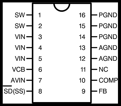
5 Pin Configuration and Functions
PW Package
16-Pin TSSOP
Top View

Pin Functions
| PIN | TYPE(1) | DESCRIPTION | |
|---|---|---|---|
| NO. | NAME | ||
| 1, 2 | SW | O | Switched-node connection, which is connected with the source of the internal high-side MOSFET. |
| 3 to 5 | VIN | I | Main power supply pin |
| 6 | VCB | I | Bootstrap capacitor connection for high-side gate drive |
| 7 | AVIN | I | Input supply voltage for control and driver circuits |
| 8 | SD(SS) | I | Shutdown and soft-start control pin. Pulling this pin below 0.3 V shuts off the regulator. A capacitor connected from this pin to ground provides a control ramp of the input current. Do not drive this pin with an external source or erroneous operation may result. |
| 9 | FB | I | Output voltage feedback input. Connected to the output voltage. |
| 10 | COMP | I | Compensation network connection. Connected to the output of the voltage error amplifier. |
| 11 | NC | G | No internal connection |
| 12 to 13 | AGND | G | Low-noise analog ground |
| 14 to 16 | PGND | G | Power ground |
(1) I = Input, O = Output, and G = Ground