SLVSES8A October 2020 – December 2020 LM5127-Q1
PRODUCTION DATA
- 1 Features
- 2 Applications
- 3 Description
- 4 Revision History
- 5 Description (continued)
- 6 Pin Configuration and Functions
- 7 Specifications
-
8 Detailed Description
- 8.1 Overview
- 8.2 Functional Block Diagram
- 8.3
Feature Description
- 8.3.1 Device Enable (EN, VCC_HOLD)
- 8.3.2 Dual Input VCC Regulator (BIAS, VCCX, VCC)
- 8.3.3 Dual Input VDD Switch (VDD, VDDX)
- 8.3.4 Device Configuration and Light Load Switching Mode Selection (CFG/MODE)
- 8.3.5 Fixed or Adjustable Output Regulation Target (VOUT, FB)
- 8.3.6 Overvoltage Protection (VOUT, FB)
- 8.3.7 Power Good Indicator (PGOOD)
- 8.3.8 Programmable Switching Frequency (RT)
- 8.3.9 External Clock Synchronization (SYNC)
- 8.3.10 Programmable Spread Spectrum (DITHER)
- 8.3.11 Programmable Soft Start (SS)
- 8.3.12 Fast Re-start using VCC_HOLD (VCC_HOLD)
- 8.3.13 Transconductance Error Amplifier and PWM (COMP)
- 8.3.14 Current Sensing and Slope Compensation (CSA, CSB)
- 8.3.15 Constant Peak Current Limit (CSA, CSB)
- 8.3.16 Maximum Duty Cycle and Minimum Controllable On-time Limits (Boost)
- 8.3.17 Bypass Mode (Boost)
- 8.3.18 Minimum Controllable On-time and Minimum Controllable Off-time Limits (Buck)
- 8.3.19 Low Dropout Mode for Extended Minimum Input Voltage (Buck)
- 8.3.20 Programmable Hiccup Mode Overload Protection (RES)
- 8.3.21 MOSFET Drivers and Hiccup Mode Fault Protection (LO, HO, HB)
- 8.3.22 Battery Monitor (BMOUT, BMIN_FIX, BMIN_PRG)
- 8.3.23 Dual-phase Interleaved Configuration for High Current Supply (CFG)
- 8.3.24 Thermal Shutdown Protection
- 8.3.25 External VCCX Supply Reduces Power Dissipation
- 8.4 Device Functional Modes
- 9 Application and Implementation
- 10Power Supply Recommendations
- 11Layout
- 12Device and Documentation Support
- 13Mechanical, Packaging, and Orderable Information
Package Options
Mechanical Data (Package|Pins)
- RGZ|48
Thermal pad, mechanical data (Package|Pins)
- RGZ|48
Orderable Information
8.3.20 Programmable Hiccup Mode Overload Protection (RES)
The device includes programmable hiccup mode overload protection which is enabled when a capacitor (CRES) is connected to the RES pin in buck configuration. The hiccup mode overload protection is disabled in boost configuration or RES is connected to VDD during initial power-on.
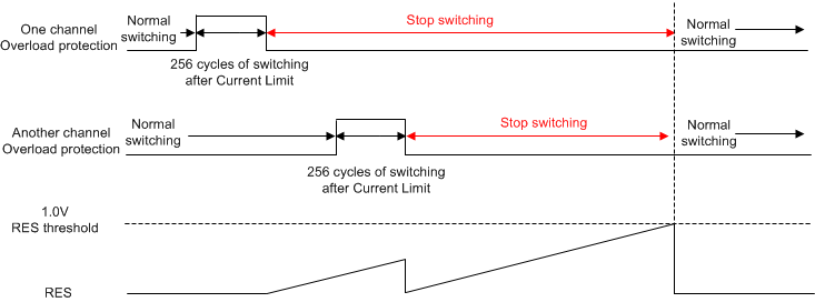
In normal operation, CRES is discharged to ground and an internal fault counter counts the clocks when cycle-by-cycle current limiting occurs. When the fault counter detects 256 cycles of switching with current limit on any buck channel, an internal hiccup mode off-timer forces the applicable channel to stop switching and starts sourcing 20 μA of current (IRES) into CRES. During this hiccup mode overload protection, the off-time before the channel restart (TRES) is programmed by CRES. During TRES, the HO and the LO outputs are disabled and CSS is charged by IRES. When the RES pin voltage reaches the RES threshold (VRESTH) , CRES is discharged by an internal RES pull-down switch, and CSS begins to charge with 30us delay. The 256 cycle fault counter is reset if eight consecutive switching cycles occur without current limit.
 Figure 8-20 Hiccup Mode Overload Protection (Single Channel
Fault)
Figure 8-20 Hiccup Mode Overload Protection (Single Channel
Fault)The device provides an independent fault counter per channel, but the RES pin is shared by all channels. The device allows that one channel is in the hiccup mode off while the other channels operate normally. In the event that multiple channels are in a fault condition, the last fault counter pulls the RES pin low and starts the RES capacitor charging cycle. Then, the multiple channels which are in the fault condition restart together when the RES pin voltage reaches VRESTH. If CH2 and CH3 are configured as an interleaved dual-phase buck, the fault counters count the fault independently, but both CH2 and CH3 stop switching and restart together.
 Figure 8-21 Hiccup Mode Overload Protection (Multiple Channel Faults)
The hiccup mode protection is also programmed during the initial configuration time. If RES is connected to VDD during the initial configuration time, the internal fault counter is disabled and the device operates with non-hiccup mode cycle-by-cycle current limit. If RES is connected to AGND, the applicable channel that detects 256 cycles of current limiting stops switching and then never restarts until the applicable channel's EN pin is toggled.
 Figure 8-22 Hiccup Mode Configuration
| RES SELECTION | SINGLE-PHASE | DUAL-PHASE | |||
|---|---|---|---|---|---|
| CH1 : BOOST | CH1 : BUCK | CH2 : BUCK | CH3 : BUCK | CH2//CH3 : BUCK | |
| RES = VDD | Cycle-by-cycle current limit | Cycle-by-cycle current limit | |||
| RES =CRES | Hiccup mode current limit | ||||
| RES = AGND | Latch-off mode current limit | ||||