SLVSES8A October 2020 – December 2020 LM5127-Q1
PRODUCTION DATA
- 1 Features
- 2 Applications
- 3 Description
- 4 Revision History
- 5 Description (continued)
- 6 Pin Configuration and Functions
- 7 Specifications
-
8 Detailed Description
- 8.1 Overview
- 8.2 Functional Block Diagram
- 8.3
Feature Description
- 8.3.1 Device Enable (EN, VCC_HOLD)
- 8.3.2 Dual Input VCC Regulator (BIAS, VCCX, VCC)
- 8.3.3 Dual Input VDD Switch (VDD, VDDX)
- 8.3.4 Device Configuration and Light Load Switching Mode Selection (CFG/MODE)
- 8.3.5 Fixed or Adjustable Output Regulation Target (VOUT, FB)
- 8.3.6 Overvoltage Protection (VOUT, FB)
- 8.3.7 Power Good Indicator (PGOOD)
- 8.3.8 Programmable Switching Frequency (RT)
- 8.3.9 External Clock Synchronization (SYNC)
- 8.3.10 Programmable Spread Spectrum (DITHER)
- 8.3.11 Programmable Soft Start (SS)
- 8.3.12 Fast Re-start using VCC_HOLD (VCC_HOLD)
- 8.3.13 Transconductance Error Amplifier and PWM (COMP)
- 8.3.14 Current Sensing and Slope Compensation (CSA, CSB)
- 8.3.15 Constant Peak Current Limit (CSA, CSB)
- 8.3.16 Maximum Duty Cycle and Minimum Controllable On-time Limits (Boost)
- 8.3.17 Bypass Mode (Boost)
- 8.3.18 Minimum Controllable On-time and Minimum Controllable Off-time Limits (Buck)
- 8.3.19 Low Dropout Mode for Extended Minimum Input Voltage (Buck)
- 8.3.20 Programmable Hiccup Mode Overload Protection (RES)
- 8.3.21 MOSFET Drivers and Hiccup Mode Fault Protection (LO, HO, HB)
- 8.3.22 Battery Monitor (BMOUT, BMIN_FIX, BMIN_PRG)
- 8.3.23 Dual-phase Interleaved Configuration for High Current Supply (CFG)
- 8.3.24 Thermal Shutdown Protection
- 8.3.25 External VCCX Supply Reduces Power Dissipation
- 8.4 Device Functional Modes
- 9 Application and Implementation
- 10Power Supply Recommendations
- 11Layout
- 12Device and Documentation Support
- 13Mechanical, Packaging, and Orderable Information
Package Options
Mechanical Data (Package|Pins)
- RGZ|48
Thermal pad, mechanical data (Package|Pins)
- RGZ|48
Orderable Information
8.3.19 Low Dropout Mode for Extended Minimum Input Voltage (Buck)
When the soft start is finished, the buck channel can enter the LDO mode if the required duty cycle is greater than the maximum duty cycle which is limited by tOFF-MIN-BUCK. During the LDO mode, the buck channels individually extends its on-time pulse to the next cycle until the PWM comparator trips. The buck channel turns off the high-side driver for 110 ns by force when the replenish pulse counter detects 15 cycles of consecutive low-side driver pulse skipping. The minimum input supply voltage which can achieve the target output voltage during the LDO mode is estimated from the following equation.
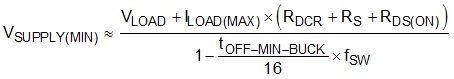
 Figure 8-19 PWM to LDO Mode Transition
| CONDITION | LIGHT LOAD SWITCHING MODE | |||
|---|---|---|---|---|
| SKIP MODE | DIODE EMULATION (USE RSS IN FPWM) | FPWM MODE | ||
| VSUPPLY >> VLOAD or at light load condition | Once HO driver turns on, the device keeps the HO driver on until the minimum peak current limit is satisfied. Random pulse skipping happens when the required peak current is less than the minimum peak current. | Random pulse skipping happens when the required on-time is less than the minimum on-time. | ||
| VSUPPLY > VLOAD | PWM operation with diode emulation | PWM operation in FPWM mode | ||
| VSUPPLY ≈ VLOAD | Enters LDO mode when the required duty cycle is greater than the maximum duty cycle limit which is defined by tOFF-MIN-BUCK. | |||
| VSUPPLY < VLOAD | Out of regulation when the required duty cycle is greater than approximately 99% | |||