SLVSES8A October 2020 – December 2020 LM5127-Q1
PRODUCTION DATA
- 1 Features
- 2 Applications
- 3 Description
- 4 Revision History
- 5 Description (continued)
- 6 Pin Configuration and Functions
- 7 Specifications
-
8 Detailed Description
- 8.1 Overview
- 8.2 Functional Block Diagram
- 8.3
Feature Description
- 8.3.1 Device Enable (EN, VCC_HOLD)
- 8.3.2 Dual Input VCC Regulator (BIAS, VCCX, VCC)
- 8.3.3 Dual Input VDD Switch (VDD, VDDX)
- 8.3.4 Device Configuration and Light Load Switching Mode Selection (CFG/MODE)
- 8.3.5 Fixed or Adjustable Output Regulation Target (VOUT, FB)
- 8.3.6 Overvoltage Protection (VOUT, FB)
- 8.3.7 Power Good Indicator (PGOOD)
- 8.3.8 Programmable Switching Frequency (RT)
- 8.3.9 External Clock Synchronization (SYNC)
- 8.3.10 Programmable Spread Spectrum (DITHER)
- 8.3.11 Programmable Soft Start (SS)
- 8.3.12 Fast Re-start using VCC_HOLD (VCC_HOLD)
- 8.3.13 Transconductance Error Amplifier and PWM (COMP)
- 8.3.14 Current Sensing and Slope Compensation (CSA, CSB)
- 8.3.15 Constant Peak Current Limit (CSA, CSB)
- 8.3.16 Maximum Duty Cycle and Minimum Controllable On-time Limits (Boost)
- 8.3.17 Bypass Mode (Boost)
- 8.3.18 Minimum Controllable On-time and Minimum Controllable Off-time Limits (Buck)
- 8.3.19 Low Dropout Mode for Extended Minimum Input Voltage (Buck)
- 8.3.20 Programmable Hiccup Mode Overload Protection (RES)
- 8.3.21 MOSFET Drivers and Hiccup Mode Fault Protection (LO, HO, HB)
- 8.3.22 Battery Monitor (BMOUT, BMIN_FIX, BMIN_PRG)
- 8.3.23 Dual-phase Interleaved Configuration for High Current Supply (CFG)
- 8.3.24 Thermal Shutdown Protection
- 8.3.25 External VCCX Supply Reduces Power Dissipation
- 8.4 Device Functional Modes
- 9 Application and Implementation
- 10Power Supply Recommendations
- 11Layout
- 12Device and Documentation Support
- 13Mechanical, Packaging, and Orderable Information
Package Options
Mechanical Data (Package|Pins)
- RGZ|48
Thermal pad, mechanical data (Package|Pins)
- RGZ|48
Orderable Information
8.3.2 Dual Input VCC Regulator (BIAS, VCCX, VCC)
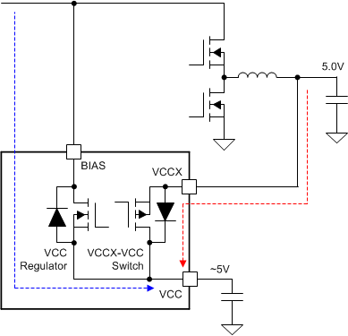
The device features a dual input VCC regulator which is sourced from either the BIAS pin or the VCCX pin. The VCC regulator is enabled 40 μs after the device is enabled.
The high voltage VCC regulator allows connecting the BIAS pin directly to supply voltages from 3.8 V to 47 V. When the BIAS pin voltage is greater than the 5-V VCC regulation target (VVCC-REG), the VCC regulator provides the 5-V regulated output. When the BIAS pin voltage is below VVCC-REG and VCCX is not used, the VCC output tracks the BIAS pin voltage with a small dropout.
The minimum VCC regulator current limit is 250 mA (IVCC-CL) during the initial configuration or when the device is in active mode. The 5-V gate charge of the external power MOSFET (QG@5V) should be selected to satisfy the following inequality.
The VCC regulator current limit is reduced to 1 mA in deep sleep mode, or when the all EN pins are less than VEN while VCC_HOLD is greater than VSYNC. The recommended minimum VCC capacitor (CVCC) value is 10 μF.
 Figure 8-1 Dual Input VCC Regulator
The battery drain in deep sleep mode and the internal power dissipation of the VCC regulator can be minimized by connecting the VCCX pin to an external power source which is greater than 4.5 V and less than 5.5 V. The VCC regulator is disabled when the VCCX pin is greater than the VCCX transition threshold (VVCCX). The internal VCCX-to-VCC switch is on when the VCC pin voltage is less than the VCCX pin voltage. If the 5-V buck output is connected to the VCCX pin, the 5-V output should be well regulated within ±10% tolerance during a load transient.
 Figure 8-2 BIAS to VCCX Transition when VCCX = VOUT2 = 5
V
Figure 8-2 BIAS to VCCX Transition when VCCX = VOUT2 = 5
VThe VCCX-to-VCC switch has no active current limit. Also, if VCCX is greater than BIAS + 0.6 V, an external reverse blocking diode is required between the input power supply and the BIAS pin. The external reverse blocking diode prevents the external VCCX supply from passing current to the BIAS pin through the VCC regulator and the VCCX-to-VCC switch. The external VCCX supply voltage can be greater than the BIAS pin voltage without the external blocking diode only if the external VCCX supply is current limited to less than 200 mA. If VCCX is not used, the VCCX pin must be grounded.
The device provides a 130 μs VVCC-UVLO-RISING-to-switching delay to ensure CVCC is fully charged by the VCC regulator before switching. If the 130-μs delay is not enough because the BIAS pin voltage rises slowly, an external RC filter can be added to the EN pin to enable the device when the BIAS pin voltage is enough high.
If CH1 is configured as a boost and the bypass operation is required, the BIAS pin should be connected to the output of the boost converter. By connecting the BIAS pin to the output of the boost converter, the start-up voltage of the boost converter is affected since the boost converter output is the converter input voltage minus one diode voltage drop before start-up, but once the converter starts up, the device allows 0.8-V minimum boost input voltage. See Section 8.3.16 for more detailed information.