SNOSDC0A October 2020 – December 2020 LM7310
PRODUCTION DATA
- 1 Features
- 2 Applications
- 3 Description
- 4 Revision History
- 5 Pin Configuration and Functions
- 6 Specifications
-
7 Detailed Description
- 7.1 Overview
- 7.2 Functional Block Diagram
- 7.3
Feature Description
- 7.3.1 Input Reverse Polarity Protection
- 7.3.2 Undervoltage Protection (UVLO & UVP)
- 7.3.3 Overvoltage Lockout (OVLO)
- 7.3.4 Inrush Current control and Fast-trip
- 7.3.5 Analog Load Current Monitor Output
- 7.3.6 Reverse Current Protection
- 7.3.7 Overtemperature Protection (OTP)
- 7.3.8 Fault Response
- 7.3.9 Power Good Indication (PG)
- 7.4 Device Functional Modes
- 8 Application and Implementation
- 9 Power Supply Recommendations
- 10Layout
- 11Device and Documentation Support
- 12Mechanical, Packaging, and Orderable Information
Package Options
Mechanical Data (Package|Pins)
- RPW|10
Thermal pad, mechanical data (Package|Pins)
Orderable Information
7.3.3 Overvoltage Lockout (OVLO)
The LM73100 allows the user to implement overvoltage lockout to protect the load from input overvoltage conditions. The OVLO comparator on the OVLO pin allows the overvoltage protection threshold to be adjusted to a user defined value. Once the voltage at the OVLO pin crosses the OVLO rising threshold VOV(R), the device turns off the power to the output. Thereafter, the devices wait for the voltage at the OVLO pin to fall below the OVLO falling threshold VOV(F) before the output power is turned ON again. The rising and falling thresholds are slightly different to provide hysterisis. The Figure 7-2 and Equation 2 below show how a resistor divider can be used to set the OVLO set point for a given input supply voltage.
 Figure 7-2 Adjustable Overvoltage
Protection
Figure 7-2 Adjustable Overvoltage
Protection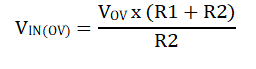
While recovering from an overvoltage event, the LM73100 starts up with inrush control (dVdt).
 Figure 7-3 LM73100 Overvoltage Lockout and
Recovery
Figure 7-3 LM73100 Overvoltage Lockout and
Recovery