SNOSDC0A October 2020 – December 2020 LM7310
PRODUCTION DATA
- 1 Features
- 2 Applications
- 3 Description
- 4 Revision History
- 5 Pin Configuration and Functions
- 6 Specifications
-
7 Detailed Description
- 7.1 Overview
- 7.2 Functional Block Diagram
- 7.3
Feature Description
- 7.3.1 Input Reverse Polarity Protection
- 7.3.2 Undervoltage Protection (UVLO & UVP)
- 7.3.3 Overvoltage Lockout (OVLO)
- 7.3.4 Inrush Current control and Fast-trip
- 7.3.5 Analog Load Current Monitor Output
- 7.3.6 Reverse Current Protection
- 7.3.7 Overtemperature Protection (OTP)
- 7.3.8 Fault Response
- 7.3.9 Power Good Indication (PG)
- 7.4 Device Functional Modes
- 8 Application and Implementation
- 9 Power Supply Recommendations
- 10Layout
- 11Device and Documentation Support
- 12Mechanical, Packaging, and Orderable Information
Package Options
Mechanical Data (Package|Pins)
- RPW|10
Thermal pad, mechanical data (Package|Pins)
Orderable Information
8.4 Priority Power MUXing
Applications having two or more power sources such as POS terminals, Tablets and other portable battery powered equipment require preference of one source to another. For example, mains power (wall-adapter) has the priority over the internal battery back-up power. These applications demand for switchover from mains power to backup power only when main input voltage falls below a user defined threshold. The LM73100 devices provide a simple solution for priority power multiplexing needs.
Figure 8-10 below shows a typical priority power multiplexing implementation using LM73100 devices. When the primary (priority) power source (IN1) is present and above the undervoltage (UVLO) threshold, the primary path device path powers the OUT bus irrespective of whether auxiliary supply voltage condition. The device in auxiliary path is held in off condition by forcing its OVLO pin to high using the EN/UVLO signal of the primary path device.
Once the primary supply voltage falls below the user-defined undervoltage threshold (UVLO), the primary path device is turned off. At the same the auxiliary, the auxiliary path device turns on and starts delivering power to the load.
In this configuration, supply overvoltage protection is not available on both channels.
The PG pins of the devices can be used as a digital indication to identify which of the 2 supplies is active and delivering power to the load.
A key consideration in power MUXing applications is the minimum voltage the output bus droops to during the switchover from one supply to another. This in turn depends on multiple factors including the output load current (ILOAD), output bus hold-up capacitance (COUT) and switchover time (tSW).
While switching from one supply rail to the other, the minimum bus voltage can be calculated using Equation 14 below. Here, the maximum switchover time (tSW) is the time taken by the device to turn on and start delivering power to the load, which is equal to the device turn on time (tON), which in turn includes the turn on delay (tD,ON) and rise time (tR) determined by the dVdt capacitor (CdVdt) and bus voltage.
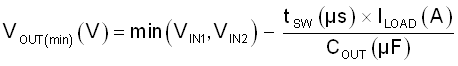
 Figure 8-10 Two Devices, Priority Power MUX
Configuration
Figure 8-10 Two Devices, Priority Power MUX
Configuration- Power MUXing can be done either between two similar rails (such as 12-V Primary & 12-V Aux; 3.3-V Primary & 3.3-V Aux) or between dissimilar rails (such as 12 V-Primary & 5-V Aux or vice versa).
- For Power MUXing cases with skewed voltage combinations, care must be taken to design circuit components on PGTH, EN/UVLO & OVLO pins for the lower voltage channel devices such that the absolute maximum ratings on those pins are not exceeded when higher voltage is present on the other channel. Also, the dVdt pin capacitor rating should be chosen based on the highest of the 2 supplies. Refer to Absolute Maximum Ratings and Recommended Operating Conditions tables for more details.