SNOSDC0A October 2020 – December 2020 LM7310
PRODUCTION DATA
- 1 Features
- 2 Applications
- 3 Description
- 4 Revision History
- 5 Pin Configuration and Functions
- 6 Specifications
-
7 Detailed Description
- 7.1 Overview
- 7.2 Functional Block Diagram
- 7.3
Feature Description
- 7.3.1 Input Reverse Polarity Protection
- 7.3.2 Undervoltage Protection (UVLO & UVP)
- 7.3.3 Overvoltage Lockout (OVLO)
- 7.3.4 Inrush Current control and Fast-trip
- 7.3.5 Analog Load Current Monitor Output
- 7.3.6 Reverse Current Protection
- 7.3.7 Overtemperature Protection (OTP)
- 7.3.8 Fault Response
- 7.3.9 Power Good Indication (PG)
- 7.4 Device Functional Modes
- 8 Application and Implementation
- 9 Power Supply Recommendations
- 10Layout
- 11Device and Documentation Support
- 12Mechanical, Packaging, and Orderable Information
Package Options
Mechanical Data (Package|Pins)
- RPW|10
Thermal pad, mechanical data (Package|Pins)
Orderable Information
7.3.5 Analog Load Current Monitor Output
The device allows the system to accurately monitor the output load current by providing an analog current sense output on the IMON pin which is proportional to the current through the FET. The user can sense the voltage (VIMON) across the RIMON to get a measure of the output load current.
Equation 5. 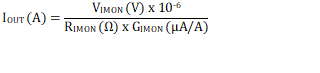
The waveform below shows the IMON signal response to a dynamically varying load profile at the output.

| VIN = 12 V, COUT = 22 μF, RIMON = 1.15 kΩ, IOUT varied dynamically between 0 A and 3.5 A |
Note:
- It's recommended to choose RIMON such that VIMON ≤ 1.5 V at the maximum DC load current.
- It's also recommended to add a zener diode on the IMON pin to clamp the voltage below 1.8 V during high current transients.
Connect IMON pin to GND if not used. Do not leave the pin floating.