SNOSDC0A October 2020 – December 2020 LM7310
PRODUCTION DATA
- 1 Features
- 2 Applications
- 3 Description
- 4 Revision History
- 5 Pin Configuration and Functions
- 6 Specifications
-
7 Detailed Description
- 7.1 Overview
- 7.2 Functional Block Diagram
- 7.3
Feature Description
- 7.3.1 Input Reverse Polarity Protection
- 7.3.2 Undervoltage Protection (UVLO & UVP)
- 7.3.3 Overvoltage Lockout (OVLO)
- 7.3.4 Inrush Current control and Fast-trip
- 7.3.5 Analog Load Current Monitor Output
- 7.3.6 Reverse Current Protection
- 7.3.7 Overtemperature Protection (OTP)
- 7.3.8 Fault Response
- 7.3.9 Power Good Indication (PG)
- 7.4 Device Functional Modes
- 8 Application and Implementation
- 9 Power Supply Recommendations
- 10Layout
- 11Device and Documentation Support
- 12Mechanical, Packaging, and Orderable Information
Package Options
Mechanical Data (Package|Pins)
- RPW|10
Thermal pad, mechanical data (Package|Pins)
Orderable Information
8.6 Parallel Operation
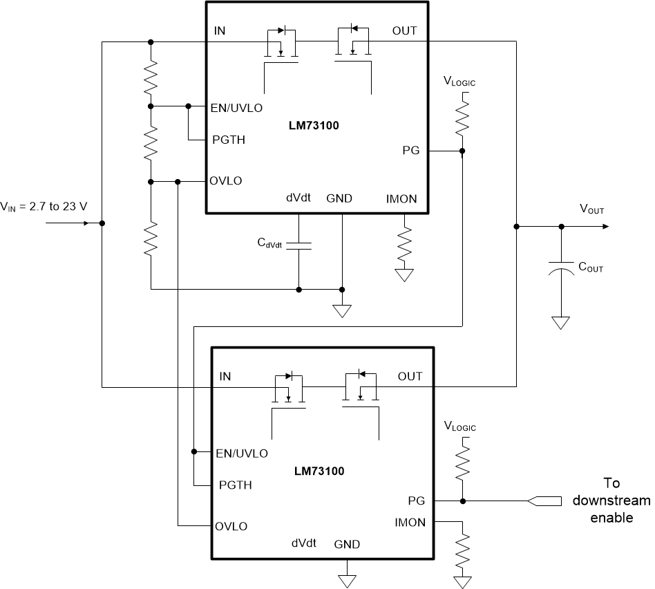
Applications which need higher steady state current can use multiple LM73100 devices connected in parallel as shown in Figure 8-14 below. In this configuration, the first device turns on initially to provide the inrush current limiting. The second device is held in an OFF state by driving its EN/UVLO pin low by the PG signal of the first device. Once the inrush sequence is complete, the first device asserts its PG pin high, allowing the second device to turn. The second device asserts its PG signal to indicate that it has turned on fully, thereby indicating to the system that the parallel combination is ready to deliver the full steady state current.
Once in steady state, the devices share current nearly equally. There could be a slight skew in the currents depending on the part-to-part variation in the RON as well as the PCB trace resistance mismatch.
 Figure 8-14 Two Devices
Connected in Parallel for Higher Steady State Current
Capability