SNVSBR8E March   2020  – October 2025 LMQ61460

PRODUCTION DATA  

  1.   1
  2. Features
  3. Applications
  4. Description
  5. Device Comparison Table
  6. Pin Configuration and Functions
  7. Specifications
    1. 6.1 Absolute Maximum Ratings
    2. 6.2 ESD Ratings
    3. 6.3 Recommended Operating Conditions
    4. 6.4 Thermal Information
    5. 6.5 Electrical Characteristics
    6. 6.6 Timing Characteristics
    7. 6.7 Systems Characteristics
    8. 6.8 Typical Characteristics
  8. Detailed Description
    1. 7.1 Overview
    2. 7.2 Functional Block Diagram
    3. 7.3 Feature Description
      1. 7.3.1  EN/SYNC Uses for Enable and VIN UVLO
      2. 7.3.2  EN/SYNC Pin Uses for Synchronization
      3. 7.3.3  Adjustable Switching Frequency
      4. 7.3.4  Clock Locking
      5. 7.3.5  PGOOD Output Operation
      6. 7.3.6  Internal LDO, VCC UVLO, and BIAS Input
      7. 7.3.7  Bootstrap Voltage and VCBOOT-UVLO (CBOOT Pin)
      8. 7.3.8  Adjustable SW Node Slew Rate
      9. 7.3.9  Spread Spectrum
      10. 7.3.10 Soft Start and Recovery From Dropout
      11. 7.3.11 Output Voltage Setting
      12. 7.3.12 Overcurrent and Short-Circuit Protection
      13. 7.3.13 Thermal Shutdown
      14. 7.3.14 Input Supply Current
    4. 7.4 Device Functional Modes
      1. 7.4.1 Shutdown Mode
      2. 7.4.2 Standby Mode
      3. 7.4.3 Active Mode
        1. 7.4.3.1 CCM Mode
        2. 7.4.3.2 Auto Mode – Light-Load Operation
          1. 7.4.3.2.1 Diode Emulation
          2. 7.4.3.2.2 Frequency Reduction
        3. 7.4.3.3 FPWM Mode – Light-Load Operation
        4. 7.4.3.4 Minimum On-Time (High Input Voltage) Operation
        5. 7.4.3.5 Dropout
  9. Application and Implementation
    1. 8.1 Application Information
    2. 8.2 Typical Application
      1. 8.2.1 Design Requirements
      2. 8.2.2 Detailed Design Procedure
        1. 8.2.2.1  Choosing the Switching Frequency
        2. 8.2.2.2  Setting the Output Voltage
        3. 8.2.2.3  Inductor Selection
        4. 8.2.2.4  Output Capacitor Selection
        5. 8.2.2.5  Input Capacitor Selection
        6. 8.2.2.6  BOOT Capacitor
        7. 8.2.2.7  BOOT Resistor
        8. 8.2.2.8  VCC
        9. 8.2.2.9  BIAS
        10. 8.2.2.10 CFF and RFF Selection
        11. 8.2.2.11 External UVLO
      3. 8.2.3 Application Curves
    3. 8.3 Power Supply Recommendations
    4. 8.4 Layout
      1. 8.4.1 Layout Guidelines
        1. 8.4.1.1 Ground and Thermal Considerations
      2. 8.4.2 Layout Example
  10. Device and Documentation Support
    1. 9.1 Documentation Support
      1. 9.1.1 Related Documentation
    2. 9.2 Receiving Notification of Documentation Updates
    3. 9.3 Support Resources
    4. 9.4 Trademarks
    5. 9.5 Electrostatic Discharge Caution
    6. 9.6 Glossary
  11. 10Revision History
  12. 11Mechanical, Packaging, and Orderable Information

Package Options

Mechanical Data (Package|Pins)
Thermal pad, mechanical data (Package|Pins)
Orderable Information

Typical Characteristics

Unless otherwise specified, VIN = 13.5 V and fSW = 400 kHz

LMQ61460 Non-Switching Input Supply Current
VFB = 1 V
Figure 6-1 Non-Switching Input Supply Current
LMQ61460 Feedback VoltageFigure 6-3 Feedback Voltage
LMQ61460 Switching Frequency Figure 6-5 Switching Frequency
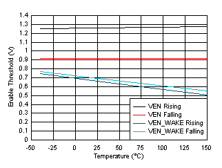
LMQ61460 Enable ThresholdsFigure 6-7 Enable Thresholds
LMQ61460 Shutdown Supply Current
VEN = 0 V
Figure 6-2 Shutdown Supply Current
LMQ61460 LMQ61460 High-Side and
                        Low-Side Current LimitsFigure 6-4 LMQ61460 High-Side and Low-Side Current Limits
LMQ61460 High-Side and Low-Side Switches RDS_ONFigure 6-6 High-Side and Low-Side Switches RDS_ON
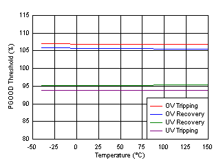
LMQ61460 PGOOD ThresholdsFigure 6-8 PGOOD Thresholds