SNVSBR8E March 2020 – October 2025 LMQ61460
PRODUCTION DATA
- 1
- 1 Features
- 2 Applications
- 3 Description
- 4 Device Comparison Table
- 5 Pin Configuration and Functions
- 6 Specifications
-
7 Detailed Description
- 7.1 Overview
- 7.2 Functional Block Diagram
- 7.3
Feature Description
- 7.3.1 EN/SYNC Uses for Enable and VIN UVLO
- 7.3.2 EN/SYNC Pin Uses for Synchronization
- 7.3.3 Adjustable Switching Frequency
- 7.3.4 Clock Locking
- 7.3.5 PGOOD Output Operation
- 7.3.6 Internal LDO, VCC UVLO, and BIAS Input
- 7.3.7 Bootstrap Voltage and VCBOOT-UVLO (CBOOT Pin)
- 7.3.8 Adjustable SW Node Slew Rate
- 7.3.9 Spread Spectrum
- 7.3.10 Soft Start and Recovery From Dropout
- 7.3.11 Output Voltage Setting
- 7.3.12 Overcurrent and Short-Circuit Protection
- 7.3.13 Thermal Shutdown
- 7.3.14 Input Supply Current
- 7.4 Device Functional Modes
- 8 Application and Implementation
- 9 Device and Documentation Support
- 10Revision History
- 11Mechanical, Packaging, and Orderable Information
Package Options
Mechanical Data (Package|Pins)
- RJR|14
Thermal pad, mechanical data (Package|Pins)
Orderable Information
3 Description
The LMQ61460 is a high-performance, DC-DC synchronous buck converter with integrated bypass capacitors. With integrated high-side and low-side MOSFETs, up to 6A of output current is delivered over a wide input range of 3.0V to 36V; tolerant of 42V, easing input surge protection design. The device implements soft recovery from dropout eliminating overshoot on the output.
LMQ61460 with ZEN 2 switcher technology is specifically designed for minimal EMI. The device incorporates pseudo-random spread spectrum, integrated bypass capacitors, adjustable SW node rise time, low-EMI VQFN-HR package featuring low switch node ringing, and optimized pinout for ease of use. The switching frequency can be synchronized between 200kHz and 2.2MHz to avoid noise sensitive frequency bands. In addition, the frequency can be selected for improved efficiency at low operating frequency or smaller design size at high operating frequency.
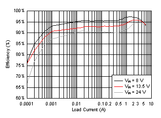
Auto mode enables frequency foldback when operating at light loads, allowing an unloaded current consumption of only 7µA (typical) and high light load efficiency. Seamless transition between PWM and PFM modes, along with very low MOSFET ON resistances and an external bias input, makes sure of exceptional efficiency across the entire load range.
| PART NUMBER | PACKAGE(1) | PACKAGE SIZE(2) |
|---|---|---|
| LMQ61460 | RJR (VQFN-HR, 14) | 4.00mm × 3.50mm |
 Simplified Schematic
 Efficiency: VOUT = 5V, fSW = 400kHz