SNVSAH2E December 2015 – August 2020 LMR23630
PRODUCTION DATA
- 1 Features
- 2 Applications
- 3 Description
- 4 Revision History
- 5 Device Comparison Table
- 6 Pin Configuration and Functions
- 7 Specifications
-
8 Detailed Description
- 8.1 Overview
- 8.2 Functional Block Diagram
- 8.3
Feature Description
- 8.3.1 Fixed Frequency Peak Current Mode Control
- 8.3.2 Adjustable Frequency
- 8.3.3 Adjustable Output Voltage
- 8.3.4 Enable/Sync
- 8.3.5 VCC, UVLO
- 8.3.6 Minimum ON-time, Minimum OFF-time and Frequency Foldback at Dropout Conditions
- 8.3.7 Power Good (PGOOD)
- 8.3.8 Internal Compensation and CFF
- 8.3.9 Bootstrap Voltage (BOOT)
- 8.3.10 Overcurrent and Short-Circuit Protection
- 8.3.11 Thermal Shutdown
- 8.4 Device Functional Modes
-
9 Application and Implementation
- 9.1 Application Information
- 9.2
Typical Applications
- 9.2.1 Design Requirements
- 9.2.2
Detailed Design Procedure
- 9.2.2.1 Custom Design With WEBENCH® Tools
- 9.2.2.2 Output Voltage Setpoint
- 9.2.2.3 Switching Frequency
- 9.2.2.4 Inductor Selection
- 9.2.2.5 Output Capacitor Selection
- 9.2.2.6 Feed-Forward Capacitor
- 9.2.2.7 Input Capacitor Selection
- 9.2.2.8 Bootstrap Capacitor Selection
- 9.2.2.9 VCC Capacitor Selection
- 9.2.2.10 Undervoltage Lockout Setpoint
- 9.2.3 Application Curves
- 10Power Supply Recommendations
- 11Layout
- 12Device and Documentation Support
- 13Mechanical, Packaging, and Orderable Information
Package Options
Refer to the PDF data sheet for device specific package drawings
Mechanical Data (Package|Pins)
- DDA|8
- DRR|12
Thermal pad, mechanical data (Package|Pins)
Orderable Information
3 Description
The LMR23630 SIMPLE SWITCHER® is an easy-to-use 36 V, 3 A synchronous step-down regulator. With a wide input range from 4 V to 36 V, it is suitable for various industrial applications for power conditioning from unregulated sources. Peak-current-mode control is employed to achieve simple control-loop compensation and cycle-by-cycle current limiting. A quiescent current of 75 μA makes the device suitable for battery-powered systems. An ultra-low 2 μA shutdown current can further prolong battery life. Internal loop compensation means that the user is free from the tedious task of loop compensation design. This also minimizes the external components. The device has an option for constant frequency FPWM mode to achieve small output-voltage ripple at light load. An extended family (HSOIC) is available in 1-A (LMR23610) and 2.5-A (LMR23625) load-current options in a pin-to-pin compatible package allowing simple, optimum PCB layout. A precision enable input allows simplification of regulator control and system power sequencing. Protection features include cycle-by-cycle current limit, hiccup-mode short-circuit protection, and thermal shutdown due to excessive power dissipation.
| PART NUMBER (1) | PACKAGE | BODY SIZE (NOM) |
|---|---|---|
| LMR23630 | HSOIC (8) | 4.89 mm × 3.90 mm |
| WSON (12) | 3.00 mm × 3.00 mm |
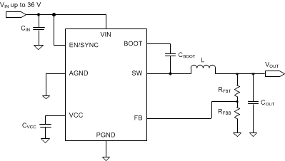
 Simplified Schematic
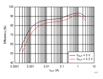
 Efficiency vs Load VIN = 12 V, PFM
Option