SNWS014D March 2004 – June 2025 LMV242 , LMV2421
PRODUCTION DATA
- 1
- 1 Features
- 2 Applications
- 3 Description
- 4 Pin Configuration and Functions
- 5 Specifications
- 6 Detailed Description
- 7 Application and Implementation
- 8 Device and Documentation Support
- 9 Revision History
- 10Mechanical, Packaging, and Orderable Information
Package Options
Refer to the PDF data sheet for device specific package drawings
Mechanical Data (Package|Pins)
- NGY|10
Thermal pad, mechanical data (Package|Pins)
Orderable Information
7.1.2.2.1 Power Control Over Wide Dynamic Range
The circuit is designed to produce a temperature-independent output power level. If the detector has a high dynamic range, the circuit precisely sets the PA output levels over a wide power range. To set a PA output power level, the reference voltage (VRAMP) is varied. To estimate the response of POUT vs VRAMP, first examine PIN vs VRAMP of the LMV242x (POUT = PIN + attenuation; see also Section 7.1.3).
The relation between PIN and VRAMPis constructed out of two curves:
- ICOMP vs VRAMP
- VOUT vs RF input power (detection curve)
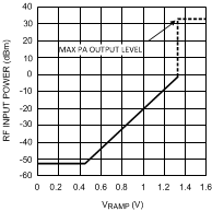
To calculate IOUT, divide the VOUT of the detection curve by the feedback resistor used for measuring. With the knowledge that ICOMP = IOUT in a closed loop, Figure 7-2 shows the resulting function of PIN vs VRAMP. Insert extra attenuation between the PA output and the LMV242x PIN to match dynamic ranges.
 Figure 7-2 PIN vs VRAMP
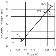
Using a closed loop to control the PA has benefits over the use of a directly controlled PA. Nonlinearity and temperature variations present in the PA transfer function do not appear in the overall transfer function, POUT vs VRAMP. Figure 7-3 gives the response of a typical closed loop. The shape of this curve is determined by the response of the controller detector. Therefore, ensure that the detector is accurate, temperature stable, and preferably linear in dB to achieve an accurately controlled output power. The only requirement for the control loop is that the gain control function of the PA is monotonic. With a linear in dB detector, the relation between VRAMP and PA output power becomes linear in dB as well, which makes system calibration easy.
 Figure 7-3 Closed-Loop Response
The response time of the loop is controlled by varying the RC time constant of the integrator. Setting the RC time constant at a low level results in fast output settling, but potentially results in ringing in the output envelope. Setting the RC time constant to a high value gives the loop good stability, but increases settling time.