SNWS014D March 2004 – June 2025 LMV242 , LMV2421
PRODUCTION DATA
- 1
- 1 Features
- 2 Applications
- 3 Description
- 4 Pin Configuration and Functions
- 5 Specifications
- 6 Detailed Description
- 7 Application and Implementation
- 8 Device and Documentation Support
- 9 Revision History
- 10Mechanical, Packaging, and Orderable Information
Package Options
Refer to the PDF data sheet for device specific package drawings
Mechanical Data (Package|Pins)
- NGY|10
Thermal pad, mechanical data (Package|Pins)
Orderable Information
5.6 Typical Characteristics
at VDD = 2.6V and TJ = 25°C (unless otherwise noted)
 Figure 5-2 Supply Current vs Supply
Voltage
 Figure 5-4 VOUT and Log Conformance vs RF
Input Power at 900MHz
 Figure 5-6 VOUT and Log Conformance vs RF
Input Power at 1900MHz
 Figure 5-8 Logarithmic Slope vs Frequency
 Figure 5-10 RF Input Impedance vs Frequency at Resistance
and Reactance
 Figure 5-12 ICOMP vs VRAMP
 Figure 5-14 Sourcing Current vs Output Voltage
 Figure 5-16 Output Voltage vs Sourcing Current
| See Section 7.1.3 for attenuation configuration between the PA output and RFIN |

| See Section 7.1.3 for attenuation configuration between the PA output and RFIN |
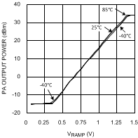
 Figure 5-22 Closed Loop DCS-1800MHz Band
 Figure 5-3 VOUT and Log Conformance vs RF
Input Power
 Figure 5-5 VOUT and Log Conformance vs RF
Input Power at 1800MHz
 Figure 5-7 VOUT and Log Conformance vs RF
Input Power at 2000MHz
 Figure 5-9 Logarithmic Intercept vs Frequency
 Figure 5-11 Gain and Phase vs Frequency
 Figure 5-13 PIN vs VRAMP
 Figure 5-15 Sinking Current vs Output Voltage
 Figure 5-17 Output Voltage vs Sinking Current
| See Section 7.1.3 for attenuation configuration between the PA output and RFIN |

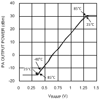
 Figure 5-23 Closed Loop PCS-1900MHz Band