SNVSAU6A November 2017 – June 2021 LP87332D
PRODUCTION DATA
- 1 Features
- 2 Applications
- 3 Description
- 4 Revision History
- 5 Pin Configuration and Functions
- 6 Specifications
-
7 Detailed Description
- 7.1 Overview
- 7.2 Functional Block Diagram
- 7.3
Feature Description
- 7.3.1 DC/DC Converters
- 7.3.2 Sync Clock Functionality
- 7.3.3 Low-Dropout Linear Regulators (LDOs)
- 7.3.4 Power-Up
- 7.3.5 Regulator Control
- 7.3.6 Enable and Disable Sequences
- 7.3.7 Device Reset Scenarios
- 7.3.8 Diagnosis and Protection Features
- 7.3.9 Operation of the GPO Signals
- 7.3.10 Digital Signal Filtering
- 7.4 Device Functional Modes
- 7.5 Programming
- 7.6
Register Maps
- 7.6.1
Register Descriptions
- 7.6.1.1 DEV_REV
- 7.6.1.2 OTP_REV
- 7.6.1.3 BUCK0_CTRL_1
- 7.6.1.4 BUCK0_CTRL_2
- 7.6.1.5 BUCK1_CTRL_1
- 7.6.1.6 BUCK1_CTRL_2
- 7.6.1.7 BUCK0_VOUT
- 7.6.1.8 BUCK1_VOUT
- 7.6.1.9 LDO0_CTRL
- 7.6.1.10 LDO1_CTRL
- 7.6.1.11 LDO0_VOUT
- 7.6.1.12 LDO1_VOUT
- 7.6.1.13 BUCK0_DELAY
- 7.6.1.14 BUCK1_DELAY
- 7.6.1.15 LDO0_DELAY
- 7.6.1.16 LDO1_DELAY
- 7.6.1.17 GPO_DELAY
- 7.6.1.18 GPO2_DELAY
- 7.6.1.19 GPO_CTRL
- 7.6.1.20 CONFIG
- 7.6.1.21 PLL_CTRL
- 7.6.1.22 PGOOD_CTRL_1
- 7.6.1.23 PGOOD_CTRL_2
- 7.6.1.24 PG_FAULT
- 7.6.1.25 RESET
- 7.6.1.26 INT_TOP_1
- 7.6.1.27 INT_TOP_2
- 7.6.1.28 INT_BUCK
- 7.6.1.29 INT_LDO
- 7.6.1.30 TOP_STAT
- 7.6.1.31 BUCK_STAT
- 7.6.1.32 LDO_STAT
- 7.6.1.33 TOP_MASK_1
- 7.6.1.34 TOP_MASK_2
- 7.6.1.35 BUCK_MASK
- 7.6.1.36 LDO_MASK
- 7.6.1.37 SEL_I_LOAD
- 7.6.1.38 I_LOAD_2
- 7.6.1.39 I_LOAD_1
- 7.6.1
Register Descriptions
- 8 Application and Implementation
- 9 Power Supply Recommendations
- 10Layout
- 11Device and Documentation Support
- 12Mechanical, Packaging, and Orderable Information
Package Options
Mechanical Data (Package|Pins)
- RHD|28
Thermal pad, mechanical data (Package|Pins)
- RHD|28
Orderable Information
7.3.6 Enable and Disable Sequences
The LP87332D device supports start-up and shutdown sequencing with programmable delays for different regulator outputs using a single EN control signal. The Buck regulator is selected for delayed control with:
- The BUCKx_EN = 1 in the BUCKx_CTRL_1 register
- The BUCKx_EN_PIN_CTRL = 1 in the BUCKx_CTRL_1 register
- The BUCKx_VSET[7:0] bits in the BUCKx_VOUT register defines the voltage when the EN pin is high
- The delay from the rising edge of the EN pin to the regulator enable is set by the BUCKx_STARTUP_DELAY[3:0] bits in the BUCKx_DELAY register.
- The delay from the falling edge of the EN pin to the regulator disable is set by the BUCKx_SHUTDOWN_DELAY[3:0] bits in the BUCKx_DELAY register.
In the same way, the LDO regulator is selected for delayed control with:
- The LDOx_EN = 1 in the LDOx_CTRL register
- The LDOx_EN_PIN_CTRL = 1 in the LDOx_CTRL register
- The LDOx_VSET[4:0] bits in the LDOx_VOUT register defines the voltage when the EN pin is high
- The delay from the rising edge of the EN pin to the regulator enable is set by the LDOx_STARTUP_DELAY[3:0] bits in the LDOx_DELAY register.
- The delay from the falling edge of the EN pin to the regulator disable is set by the LDOx_SHUTDOWN_DELAY[3:0] bits in the LDOx_DELAY register.
The GPO and GPO2 digital output signals can be also controlled as a part of start-up and shutdown sequencing with the following settings:
- GPOx_EN = 1 in GPO_CTRL register
- GPOx_EN_PIN_CTRL = 1 in GPO_CTRL register
- The delay from the rising edge of the EN pin to the rising edge of the GPO or GPO2 signal is set by the GPOx_STARTUP_DELAY[3:0] bits in the GPOx_DELAY register.
- The delay from the falling edge of the EN pin to the falling edge of the GPO or GPO2 signal is set by the GPOx_SHUTDOWN_DELAY[3:0] bits in the GPOx_DELAY register.
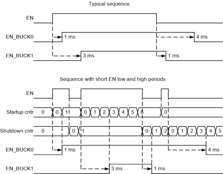
An example of the start-up and shutdown sequences for the buck regulators are shown in Figure 7-7. The start-up and shutdown delays for the Buck0 regulator are 1 ms and 4 ms, and for the Buck1 regulator the start-up and shutdown delays are 3 ms and 1 ms. The delay settings are only used for enable or disable control with the EN signal.
 Figure 7-7 Start-Up and Shutdown Sequencing