SNVSCJ1 August 2023 LV5144
PRODUCTION DATA
- 1
- 1 Features
- 2 Applications
- 3 Description
- 4 Revision History
- 5 Description (continued)
- 6 Pin Configuration and Functions
- 7 Specifications
-
8 Detailed Description
- 8.1 Overview
- 8.2 Functional Block Diagram
- 8.3
Feature Description
- 8.3.1 Input Range (VIN)
- 8.3.2 Output Voltage Setpoint and Accuracy (FB)
- 8.3.3 High-Voltage Bias Supply Regulator (VCC)
- 8.3.4 Precision Enable (EN/UVLO)
- 8.3.5 Power Good Monitor (PGOOD)
- 8.3.6 Switching Frequency (RT, SYNCIN)
- 8.3.7 Configurable Soft Start (SS/TRK)
- 8.3.8 Voltage-Mode Control (COMP)
- 8.3.9 Gate Drivers (LO, HO)
- 8.3.10 Current Sensing and Overcurrent Protection (ILIM)
- 8.3.11 OCP Duty Cycle Limiter
- 8.4 Device Functional Modes
- 9 Application and Implementation
- 10Device and Documentation Support
- 11Mechanical, Packaging, and Orderable Information
Package Options
Mechanical Data (Package|Pins)
- RGY|20
Thermal pad, mechanical data (Package|Pins)
- RGY|20
Orderable Information
8.3.4 Precision Enable (EN/UVLO)
The EN/UVLO input supports adjustable input undervoltage lockout (UVLO) with hysteresis programmed by the resistor values for application specific power-up and power-down requirements. EN/UVLO connects to a comparator-based input referenced to a 1.2-V bandgap voltage. An external logic signal can be used to drive the EN/UVLO input to toggle the output ON and OFF and for system sequencing or protection. The simplest way to enable the operation of the LV5144 is to connect EN/UVLO directly to VIN. This allows self start-up of the LV5144 when VCC is within its valid operating range. However, many applications benefit from using a resistor divider RUV1 and RUV2 as shown in Figure 8-3 to establish a precision UVLO level.
Use Equation 1 and Equation 2 to calculate the UVLO resistors given the required input turn-on and turn-off voltages.
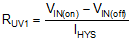
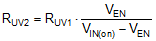
 Figure 8-3 Programmable Input Voltage
UVLO Turn-on and Turn-off
Figure 8-3 Programmable Input Voltage
UVLO Turn-on and Turn-offThe LV5144 enters a low IQ shutdown mode when EN/UVLO is pulled below approximately 0.4 V. The internal LDO regulator powers off and the internal bias supply rail collapses, shutting down the bias currents of the LV5144. The LV5144 operates in standby mode when the EN/UVLO voltage is between the hard shutdown and precision enable (standby) thresholds.