SNVSCJ1 August 2023 LV5144
PRODUCTION DATA
- 1
- 1 Features
- 2 Applications
- 3 Description
- 4 Revision History
- 5 Description (continued)
- 6 Pin Configuration and Functions
- 7 Specifications
-
8 Detailed Description
- 8.1 Overview
- 8.2 Functional Block Diagram
- 8.3
Feature Description
- 8.3.1 Input Range (VIN)
- 8.3.2 Output Voltage Setpoint and Accuracy (FB)
- 8.3.3 High-Voltage Bias Supply Regulator (VCC)
- 8.3.4 Precision Enable (EN/UVLO)
- 8.3.5 Power Good Monitor (PGOOD)
- 8.3.6 Switching Frequency (RT, SYNCIN)
- 8.3.7 Configurable Soft Start (SS/TRK)
- 8.3.8 Voltage-Mode Control (COMP)
- 8.3.9 Gate Drivers (LO, HO)
- 8.3.10 Current Sensing and Overcurrent Protection (ILIM)
- 8.3.11 OCP Duty Cycle Limiter
- 8.4 Device Functional Modes
- 9 Application and Implementation
- 10Device and Documentation Support
- 11Mechanical, Packaging, and Orderable Information
Package Options
Mechanical Data (Package|Pins)
- RGY|20
Thermal pad, mechanical data (Package|Pins)
- RGY|20
Orderable Information
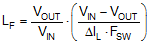
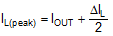
9.1.2.1 Inductor
For most applications, choose an inductance such that the inductor ripple current, ΔIL, is between 30% and 40% of the maximum DC output current at nominal input voltage. Choose the inductance using Equation 7 based on a peak inductor current given by Equation 8.
Check the inductor data sheet to ensure that the saturation current of the inductor is well above the peak inductor current of a particular design. Ferrite designs have very low core loss and are preferred at high switching frequencies, so design goals can then concentrate on copper loss and preventing saturation. Low inductor core loss is evidenced by reduced no-load input current and higher light-load efficiency. However, ferrite core materials exhibit a hard saturation characteristic and the inductance collapses abruptly when the saturation current is exceeded. This results in an abrupt increase in inductor ripple current, higher output voltage ripple, not to mention reduced efficiency and compromised reliability. Note that the saturation current of an inductor generally decreases as its core temperature increases. Of course, accurate overcurrent protection is key to avoiding inductor saturation.