SBOSA11E March 2020 – December 2023 OPA206 , OPA2206 , OPA4206
PRODUCTION DATA
- 1
- 1 Features
- 2 Applications
- 3 Description
- 4 Pin Configuration and Functions
- 5 Specifications
- 6 Parameter Measurement Information
- 7 Detailed Description
- 8 Application and Implementation
- 9 Device and Documentation Support
- 10Revision History
- 11Mechanical, Packaging, and Orderable Information
Package Options
Refer to the PDF data sheet for device specific package drawings
Mechanical Data (Package|Pins)
- D|8
- DGK|8
Thermal pad, mechanical data (Package|Pins)
Orderable Information
7.3.1 Input Overvoltage Protection
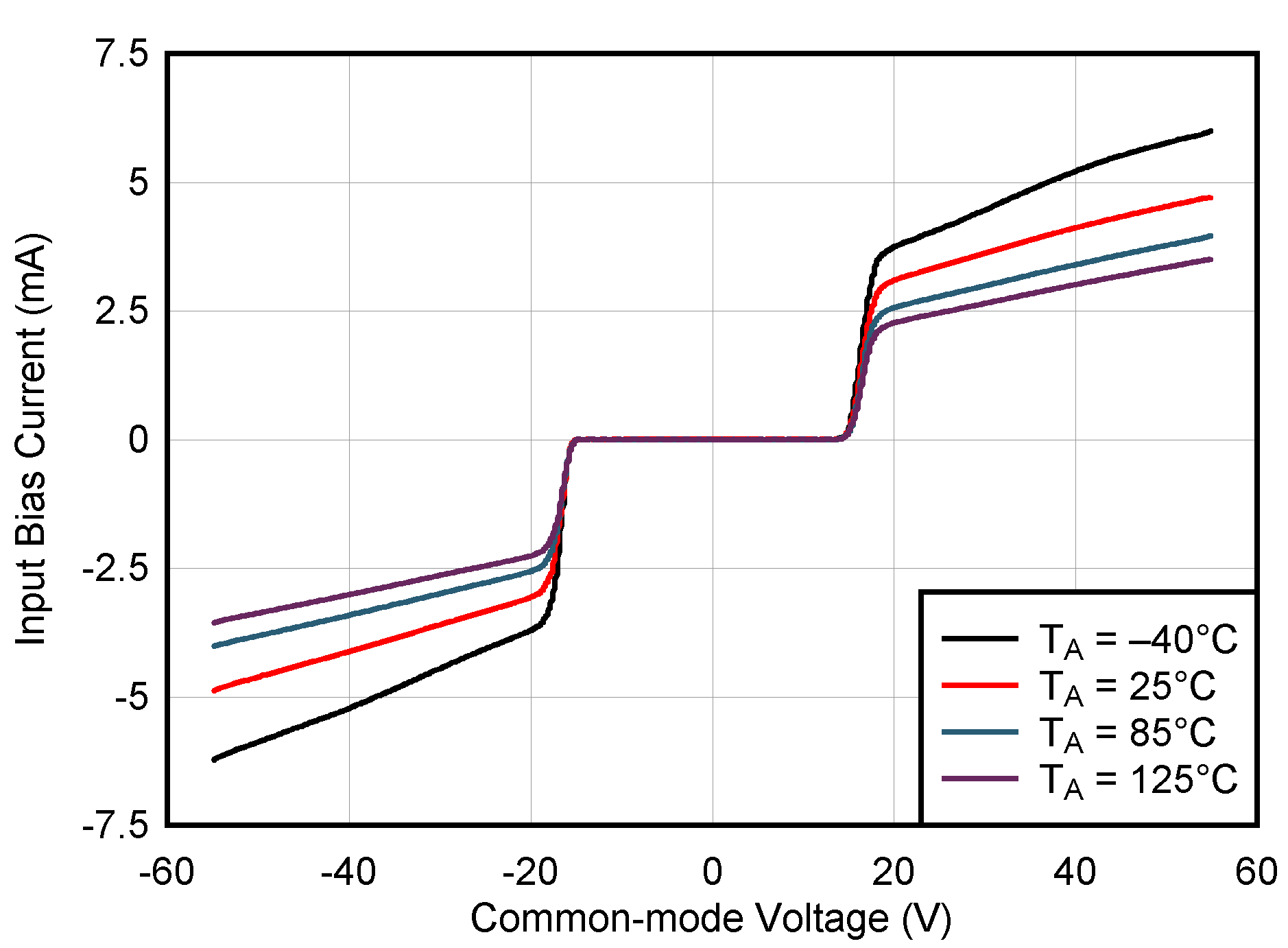
The inputs of the OPAx206 are individually protected for voltages up to ±40 V beyond either supply. For example, a common-mode voltage anywhere between –55 V and +55 V does not cause damage when powered from ±15-V supplies. Internal circuitry on each input provides low series impedance under normal signal conditions thus maintaining high performance under normal operating conditions. If the input is overloaded, the protection circuitry limits the input current to a value of approximately 4.8 mA.
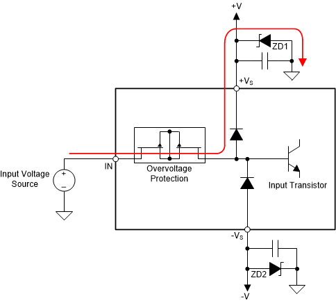
During an input overvoltage condition, current flows through the input protection diodes into the power supplies, as shown in Figure 7-1. If the power supplies are unable to sink current, then Zener diode clamps (ZD1 and ZD2) must be placed on the power supplies to provide a current pathway to ground. Figure 7-2 shows that during an overvoltage condition, the input bias current of the inputs increase.
 Figure 7-1 OPAx206
Input Overvoltage Current Path
Figure 7-1 OPAx206
Input Overvoltage Current PathFigure 7-2 shows the input current for input voltages from –55 V to +55 V when the OPAx206 are powered by ±15-V supplies.

| VS = ±15 V |